Continue to Site

Welcome to our site!

Electro Tech is an online community (with over 170,000 members) who enjoy talking about and building electronic circuits, projects and gadgets. To participate you need to register. Registration is free. Click here to register now.

  • Welcome to our site! Electro Tech is an online community (with over 170,000 members) who enjoy talking about and building electronic circuits, projects and gadgets. To participate you need to register. Registration is free. Click here to register now.

Designing differerntial Signal modulator

Status
Not open for further replies.

Alex_bam

New Member
Hello, 1.JPG1.JPG2.JPG
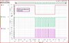
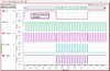
I would like your suggestion on my first design Differential signal modulator [simulation attached].

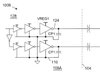
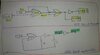
Before jumping into design let me highlight my objective. I am differentiating a control signal of 1MHz and then modulating it with carrier frequency 15MHz(not limited to this specific value but for testing). The whole modulator needs to be integrated on a silicon substrate, in other words, the design should comply with IC design regulations i.e. occupy less space, power-efficient, and simple. The current design consumes 5.6mW power.

So I would request suggestions who had experience in a related field, that

1-How can I further improve this design?

2-Is there other alternatives design that would be much better than this one?


Your suggestions and comments will be highly appreciated. Thanks

1.JPG

2.JPG
 
i'm not sure what you are trying to accomplish here, but the outputs aren't actually differential.... you wouldn't be able to effectively drive a split primary winding on a transformer for instance. what you have is alternating active outputs, which could be used for instance to drive two LEDs, one at a time... an actual differential output would have one output, for instance V_diff_1, and an inverted copy of it as the other output...so whenever V_diff_1 is 0V, the other output is 5V, and vice-versa. both outputs would be putting out pulses (one positive-going, the other negative-going), or "resting (one at 0V, the other at 5V)
 
i'm not sure what you are trying to accomplish here, but the outputs aren't actually differential.... you wouldn't be able to effectively drive a split primary winding on a transformer for instance. what you have is alternating active outputs, which could be used for instance to drive two LEDs, one at a time... an actual differential output would have one output, for instance V_diff_1, and an inverted copy of it as the other output...so whenever V_diff_1 is 0V, the other output is 5V, and vice-versa. both outputs would be putting out pulses (one positive-going, the other negative-going), or "resting (one at 0V, the other at 5V)

Thanks for your suggestion. Maybe I did not translate my issue properly. I am trying to implement the idea mentioned in
US Patent: US 7923710B2 "Digital isolation with communication across an isolation barrier". I already implemented capacitive coupling isolation on IC with a single-ended signal by using the oscillator schematic mentioned in my question. To implement capacitive isolation with a differential signal I found this US patent.

If I understood correctly. In the patent, they use NOT gate to invert/differentiate control signal and then modulate inverted signals with modulators. The coupling capacitor coupled modulated signal by providing isolation on a silicon substrate.

The reason for using NAND gate in single-ended signal setup: Due to the NAND gate, it only modulates when the control signal is high. This is because the control signal is held low when no communications are occurring. The modulator is idle when no communication is occurring, making this modulator design power efficient.
 

Attachments

  • 3.JPG
    3.JPG
    17.5 KB · Views: 324
run your carrier and data stream through a XOR gate, then take the output, and run it through an inverter... the XOR output would be the noninverted signal, and the inverter output would be the inverted signal... now you have differential signals on a modulated carrier. the two signals could then drive buffer amplifiers, and the outputs of the buffer amplifiers would each drive one half of a dipole antenna. you can still gate the signal with a single NAND or AND gate after the XOR gate to idle the transmitter.
 
Last edited:
run your carrier and data stream through a XOR gate, then take the output, and run it through an inverter... the XOR output would be the noninverted signal, and the inverter output would be the inverted signal... now you have differential signals on a modulated carrier. the two signals could then drive buffer amplifiers, and the outputs of the buffer amplifiers would each drive one half of a dipole antenna. you can still gate the signal with a single NAND or AND gate after the XOR gate to idle the transmitter.

Thanks for your suggestion. I implement two different designs (the one you suggested and one based on my previous design)[attahed]. I would like to discuss:

1-Could you please confirm the first drawing, Is this corresponds to what you suggested?
2-Could you please elaborate on the reason for using the XOR gate in your suggested design?
3-Is the XOR gate still necessary after comparing the two mentioned designs although we can get the same result from both? Please correct me if I am wrong.
4-What is your assessment /views about my design?

Thanks for your help and cooperation.
 

Attachments

  • 20210223_140540.jpg
    20210223_140540.jpg
    136.1 KB · Views: 297
  • NOR.JPG
    NOR.JPG
    232.7 KB · Views: 301
  • XOR.JPG
    XOR.JPG
    265.1 KB · Views: 310
since basically you are transmitting across open space (isolation barrier can be an air gap, or apiece of insulating material, same thing electrically), you want to treat this as a radio link.

1 your first drawing is similar to what i suggested but not quite the same

2 the XOR gate inverts the phase of the carrier instead of using on-off keying, and eliminates the DC component (or "keying thump") after passing the signal through a capacitor... the phase inversion rather than on-off keying reduces the signal bandwidth.. a receiver for this signal is more complex, but the on-off keying is more subject to noise and interference from outside sources. the output of the XOR gate is a BPSK modulated radio wave. a receiver using a phase-locked loop will easily recover the original data, and the phase detector of the PLL will ignore most noise as long as the transmitted signal is present.

3 the first design you presented wasn't really differential, and your NOR output signal is on-off keying with differential outputs, and may be suitable for capacitive coupling to an isolated part of the same chip. if however you were looking for this device to have some radio applications, where the receiver is more distant, the XOR modulator with BPSK modulation is probably a more efficient way to get data across a link. the differential output (such as in XOR.JPG) could directly feed a dipole antenna. since the output is a raww digital signal, a lot of filtering would be required between the modulator and the antenna to turn the carrier into a sine wave, but it shouldn't be really complicated. it would be well suited for a HIFER transmitter where low output power and narrow bandwidth are both required. HIFER transmitters operate in the 13.55Mhz ISM band.

4 what you have in post #6, will work through capacitive isolation on the same chip as the receiver no problem.

when i get home from work i think i can clean some of it up and simplify it for you, as well as lay out a schematic of what i had in mind for a radio link (which is what i thought you originally had in mind)...

Thank you so much for your detail explanation.

1-I should clarify my target, My aim is to design capacitive coupling isolation of control signal on IC to drive isolated gate driver with the limitation of having minimum or no electromagnetic field (means avoiding inductive or transformer-based isolation technique).

2- From your explanation (in point 3 and 4 of post#7), I understood that NOR based modulator will be suitable for on-chip capacitive isolation, however, an XOR-based modulator will be preferable for radio wave application. So I can go for NOR based modulator for the on-chip cap isolation technique. Correct me if I got it wrong?

3-It would be nice of you if you could suggest to me a demodulator for a differential signal for NOR based modulator. Actually, I searched online but ended up with no clear design. Although I am still searching for an appropriate demodulator design compatible with IC and magnetic field constrains.

Thanks.
 
Status
Not open for further replies.

Latest threads

New Articles From Microcontroller Tips

Back
Top