Offset voltage is ALWAYS there, and is not produced by external components (although I assume it could be affected by them). It comes from the halves of the differential inputs inside the op-amp not being perfectly matched.
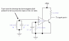
However, a SECOND offset voltage can be made because the bias current of the two op-amp inputs is travelling through different resistances. You can correct for this by adding resistors/capacitors to the non-inverting input to make the bias currnts travel through the same resistance (and therefore get common-mode rejected by the op-amp differential inputs). That is probably why you connected the non-inverting input to ground through a resistor rather than just connecting it directly to ground. The resistor is there to make both opamp inputs see the same impedence. This offset voltage, however, is not in the datasheets because it depends on the components around the op-amp.