hi C,
As I understand the datasheet, I believe the SX must in Standby when programming.
E
EDIT:
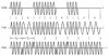
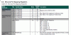
Are you following the TX procedure for OOK [On Off Keying] as per this image clip.
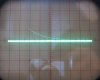
I would expect the TX RF output to be zero when not transmitting or when the transmitted data BIT is a '0' and full TX RF when the BIT is a '1'
https://en.wikipedia.org/wiki/On-off_keying
As I understand the datasheet, I believe the SX must in Standby when programming.
E
EDIT:
Are you following the TX procedure for OOK [On Off Keying] as per this image clip.
I would expect the TX RF output to be zero when not transmitting or when the transmitted data BIT is a '0' and full TX RF when the BIT is a '1'
https://en.wikipedia.org/wiki/On-off_keying
Attachments
Last edited:

")
 With the supplied coiled spring aerial, 100mtr range after a quick test. I've updated Post #1
")
