Continue to Site

Welcome to our site!

Electro Tech is an online community (with over 170,000 members) who enjoy talking about and building electronic circuits, projects and gadgets. To participate you need to register. Registration is free. Click here to register now.

  • Welcome to our site! Electro Tech is an online community (with over 170,000 members) who enjoy talking about and building electronic circuits, projects and gadgets. To participate you need to register. Registration is free. Click here to register now.

Damaged pad on laptop motherboard

Status
Not open for further replies.
IMG_9481.JPG
 
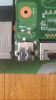
If this is the area of concern:
upload_2017-12-27_6-19-45.png


I would do some testing before trying to "replace" the pads. It is a multilayer board and at a minimum, contact on both visible sides can be important. It also looks like the lower pad is connected to the upper on each side. It looks like there is enough pad left on at least 3 of the 4 and perhaps all four to get a solder joint. I am assuming the component was on the side that is showing.

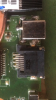
What does the other side look like? Presumably, that side looks OK.

I would confirm those assumptions by using an ohmmeter or conductivity tester on the pads. No need to poke through the solder mask at this time.

If the electrical connections are OK, I might do a little repair by tinning the component side a little, insert the new connector, solder from the back side as usual, and then check the top side to see if it got a little solder flow around the pins. Regardless of that, I would go ahead and test it. If it doesn't work, then I would consider trying to get a little solder on the top side; however, if the electrical checks are all OK, I don't think that will be necessary.
 
Thank you for your response. Yes that is the area I was questioning and the powerjack fits to that side. The other side of the board has no damage. I have checked the board with a multimeter and the connections all appear to be ok where the pads remain. I will try to tin the side that is missing and install the new powerjack. Thanks again for the advice. My first attempt at desoldering.
 
Be sure to add a very thin film of flux in the area you are trying to re-tin. By very thin, I will smear on my paste with something like a Q-tip, then wipe it off with a towel.

Good luck and please let us know how it turns out.
 
Are you able to explain how to tin the edge please? I'm new to this sorry. From what I understand is you need to heat the part you want the solder to bond to. In my case because the pad is partially missing how do I get the solder to stay in place?
 
You cannot tin bare PCB material. The only purpose of tinning any remaining copper on the top is to facilitate the solder flowing to the remnant of copper there. When I deal with homemade boards without plated through holes, I will often solder on top as close as I can get. Then when soldering on the bottom , the heat will allow me to re-seat the part.

Here is an example with a bridge rectifier. I soldered on top, then when soldering the bottom, I re-seated it to be flush with the PCB. I use leaded solder, which may make doing that a little easier.

upload_2017-12-27_17-23-22.png


Your damaged pads on the top do not look that bad. Do the best you can and see if it works.

John
 
I have soldered the new powerjack on an it works. The solder has gone onto one of the component pins next to the powerjack, hopefully this won't cause any issues. Thanks again for your help.
 

Attachments

  • IMG_9492.PNG
    IMG_9492.PNG
    1.4 MB · Views: 230
  • IMG_9493.PNG
    IMG_9493.PNG
    1.4 MB · Views: 223
Congratulations. If this is that pin you mention, it already had solder on it originally. What is important is that it works.
upload_2017-12-28_0-33-49.png


John
 
Status
Not open for further replies.

Latest threads

New Articles From Microcontroller Tips

Back
Top