Continue to Site

Welcome to our site!

Electro Tech is an online community (with over 170,000 members) who enjoy talking about and building electronic circuits, projects and gadgets. To participate you need to register. Registration is free. Click here to register now.

  • Welcome to our site! Electro Tech is an online community (with over 170,000 members) who enjoy talking about and building electronic circuits, projects and gadgets. To participate you need to register. Registration is free. Click here to register now.

CS amplifier.

Status
Not open for further replies.

alphacat

New Member
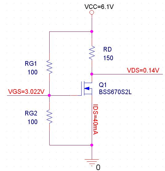
I built a CS amplifier today, using a **broken link removed** (N-ch MOSFET).

I got the following results (in RED).

I really dont understand why the MOSFET's VDS was so low.
The voltage drop on RD was 6V, its very weird.
Even when I changed RD from 150Ω to 47KΩ, RD's voltage drop was still 6V.

Why did the MOSFET keep being in the linear region?
I waned to get it into its saturation region.

Could it be because of the diode its got connected between its D-S channel?


cs-amplifier-jpg.35039
 

Attachments

  • CS amplifier.JPG
    CS amplifier.JPG
    24.9 KB · Views: 525
The device is in a saturated condition. Changing the vale of the drain resistor does not chnage this condition.

The linear region would be have a larger vlaue for VDS.
 
Your question is easy: 40mA * 150 = 6V. 6.1V(VDD) - 6V = .1V. If you want active region (satruation) you need either higher VDD, lower drain resistor, or change the gate bias (lower)
 
I see, thank you.
I have 2 questions please.

1. At first, I picked RG1=RG2=47Kohm, and when I powered-up the circuit, VGS was not 3.05V but it was less than 0.5V.
I measured the resistance of RG2 when it was still connected to the circuit, and the multimeter read 3Kohm! its like the Gate-source had a resistance of 3Kohm.
Could you please explain this phenomenon to me?

2. If I decreased VDD to 1V, so VGS=0.5V<VTn.
Should I have seen VDS = VDD? (since no current would have flown throught RD).

Thanks.

--
By the way, perhaps "Are our children learning?" is less rare a question ;)
 
Last edited:
The quote in my signature was taken verbatim from one of my country's great leaders.

You can't measure the value of RG2 in your circuit with any accuracy. If you resistance meter uses voltage higher than the transistor's threshold voltage, you turn on the transistor.

If VGS of .5 volts is less than Vt, then you should see VGS=VDD.
 
The quote in my signature was taken verbatim from one of my country's great leaders.
I agree :)

You can't measure the value of RG2 in your circuit with any accuracy. If you resistance meter uses voltage higher than the transistor's threshold voltage, you turn on the transistor.
Well, the fact was that when using RG1=RG2=47KΩ, the VGS was equal to VDD/2, but was equal to ~0.4V.
I didnt understand your sentence about the voltage the multimeter uses, could you explain how its got to do with the problem?


If VGS of .5 volts is less than Vt, then you should see VGS=VDD.
You mean VDS=VDD, right?
 
You mean VDS=VDD, right?
Right. Too easy to get those mixed up.

I didnt understand your sentence about the voltage the multimeter uses, could you explain how its got to do with the problem?

If you're using a multimeter with resistance measurement selected across R2, you're applying a voltage from the meter which can forward bias Q1, which effectively puts R1 and the DS of Q1 in parallel with R2. I can't begin to explain the 0.4V you get with R1=R1=47K. Something seems wrong there.
 
Last edited:
Right. Too easy to get those mixed up.


If you're using a multimeter with resistance measurement selected across R2, you're applying a voltage from the meter which can forward bias Q1, which effectively puts R1 and the DS of Q1 in parallel with R2. I can't begin to explain the 0.4V you get with R1=R1=47K. Something seems wrong there.

Well, I really measured the voltage on RG2 (VGS) and it was ~0.4V when RG1=RG2=47kOhm.
But when I picked up RG1=RG2=100ohm, then VGS was VDD/2.
I dont get it also.

By the way, what is usually the zenner voltage of such D-S diodes?
It wasnt specified in the datasheet.
 
There isn't a zener voltage is the D-S of a mosfet. They are electrically isolated. A voltage that breaks down the barrier would most likely destroy the device.
 
I was wondering whats its Zener voltage, it isnt specified in the datasheet, so whats the usual zener voltage in such D-S zener diode?
 
There isn't a zener voltage. That's why it's not specified on the data sheet.
 
You will notice on the spec sheet, under the heading "Feature", it says "Avalanche rated". Then a little further down is a single pulse avalanche energy rating of 8.1 millijoules.

What that means is that it's ok to use the body diode like a zener, and the device won't be harmed.

If you were to put a .1 henry inductor in series with the drain and a power supply of, say, 12 volts, and apply a pulse to the gate to turn on the device for about 33 milliseconds, the current in the inductor would ramp up to .4 amps.

Then, let the gate drive go to zero. The device will turn off, and the voltage at the drain will rise until the body diode breaks down in zener mode. The energy stored in the inductor when the device is turned off is 8 millijoules, and that energy will be dissipated as heat in the device.

What the spec sheet is saying is that you can do that without hurting the device, if the starting temperature is 25 degrees, and if you let it cool down to 25 degrees before you do it again.

For use where the body diode is conducting current continuously in zener mode, you must see to it that the dissipation remains within the Ptot rating of the device. That is, the product of the zener current and the zener breakdown voltage must remain less that .36 watts (at 25 degrees; an infinite heat sink would have to be provided to keep the temperature at 25 degrees if the device were dissipating .36 watts). If the device temperature can rise when it's dissipating power (as is the usual case), then you must keep the dissipation below the value shown in the figure 1 graph for a particular device temperature. The thermal resistance parameter, Rthjs, can be used to help determine the allowable zener current at various temperatures.

Now, as to your question about just what the zener voltage is. Typically, for MOSFETs whose body diode is specified for use as a zener, the breakdown is just a little higher than the Vds rating. I would expect it to be in the range of 65 to 80 volts. You could easily measure it. Short the gate to source, and put a 10k ohm resistor and a variable power supply (capable of 100 volts output) in series with the device's drain to source terminals with the proper polarity--positive on the drain. Slowly turn up the supply while monitoring the voltage across the device; the voltage will stop rising when you reach the zener breakdown voltage. Don't keep increasing the voltage much past the point where you can tell that you've reached the zener breakdown voltage, or you may overheat the device.

An interesting aspect of the ability of a MOSFET's body diode to act as a zener diode is that if you need a really high power zener, you can buy a high power MOSFET (some can dissipate 250 watts or more in a TO220 case), short the gate to source and use it as a 250 watt zener. You can't buy a regular 250 watt zener as cheaply as you can buy a high power MOSFET.

Also, as long as you stay below the zener breakdown voltage of the MOSFET's body diode, you can short the gate to source and use the diode as an ordinary rectifier diode. Again, you can buy a 50 volt power MOSFET with a current rating greater than 100 amps for a few dollars. You could use 4 of them to make a 100 amp bridge rectifier for a high current power supply.
 
Last edited:
My apologies to the OP. I thought we were talking about the G-S of the MOSFET, after our discussion about why the gate was not measuring what he expected. I missed the point that we had shifted the discussion to the D-S protection diode.
 
Status
Not open for further replies.

New Articles From Microcontroller Tips

Back
Top