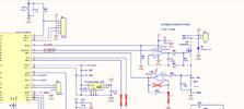
The power FET may have quite a high gate capacitance, which limits the rate of change with just an opamp feeding it.
Especially with R5 in place. This is a common mistake when an inexperienced designer uses a power MOSFET in a linear circuit, having seen them only or mostly in switching power circuits.
In a switching power supply, lead and pcb trace inductance and gate capacitance can form an LC circuit that rings after a fast edge goes through it. Power MOSFET gates are driven with a very fast, high-current square wave to overpower the gate capacitance. This forces the FET to go from completely "on" (fully enhanced) to completely off very quickly, reducing the amount of time it spends in its linear region where it dissipates wasted heat. It's all about efficiency.
R5 and the gate capacitance form a single-stage R-C lowpass filter. This limits the gate capacitor voltage rate of change, removing or decreasing the high frequency harmonics from the voltage edge energy spectrum, greatly reducing the ringing waveform amplitude. Without it, a power stage switching at 50 kHz can ring so badly at 250 MHz that it fails RF noise compliance testing.
For example, a gate capacitance of 1 nF (not a particularly large value) with a 100 ohm resistor is a corner frequency of 1.6 MHz. This is 5 ocatves above a switching frequency of 50 kHz, and has no visible effect on the driving waveform. BUT - At 160 MHz, the harmonic attenuation is 40 dB. So how easy is it for this problem to occur? Very. The inductance needed to resonate with a 1 nF capacitor at 160 MHz is only 1 nH. That's not much.
The existence of R5 came about for a reason, but that reason is being lost. In a linear circuit such as a CC source, it does zero good and can complicate things.
ak