Continue to Site

Welcome to our site!

Electro Tech is an online community (with over 170,000 members) who enjoy talking about and building electronic circuits, projects and gadgets. To participate you need to register. Registration is free. Click here to register now.

  • Welcome to our site! Electro Tech is an online community (with over 170,000 members) who enjoy talking about and building electronic circuits, projects and gadgets. To participate you need to register. Registration is free. Click here to register now.

complicated single side PCB layouts!

Status
Not open for further replies.

computer

New Member
Grr,

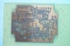
I have a circuit I'd like to get made on to some PCBs and I can't find any low-cost places I can get it made up properly in the UK, so I'm going to have to try and etch it myself using either a steady hand or some sort of press-n-peel.

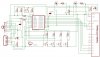
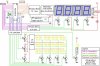
The schematic is attached and as you can see its quite compled. The main bits are the PICAXE and the LCD. Also a 6 way header and an ethernet socket.

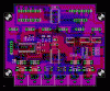
Anyone here think that it's possible to get that done on two single side copper boards, 65x65mm max? If so what do you suggest for layout the best? I will use ribbon cable to connect the two boards. The top one needs to have 16 pins at 2.54mm spacing along the bottom-left edge somewhere for the LCD (14 pins + 2 for the backlight - shown by LED1 on the diagram).

Any tips are welcomed. Many autorouter tools fail to manage to route it!
 

Attachments

  • schematic.jpeg
    schematic.jpeg
    113 KB · Views: 1,544
One thing I've learned is that the autorouter tool is just that... a TOOL. I've never been able to use autorouter alone, except for very simple boards. Usually I can get the autorouter to pull off about 80-90% of the connections, and I use that as a starting point... adding and removing traces as I see fit. (autorouting usually ends up with a few totally stupid traces, such as running all the way around the edge of the board to reach a pin 1/4 inch away, instead of just using a jumper)
I think the biggest reason autorouter isn't a perfect solution is that it depends heavily on where you place the parts. unless you can find a package that does placement AND routing automatically, then you have to experiment.

it looks like you're using eagle. if you send me your SCH file maybe I can work something out with it... honestly it doesn't look that complicated... take a look at: https://eegeek.net/electronics/projects/function_generator

bear in mind that a lot of the connections in that diagram are done by labeling the nets, rather than running the wires, to make the diagram less cluttered... such as the 12 wires going from the lower part of the PIC to the chip shown on the right. Autorouter certainly couldn't handle the layout on its own, but as you can see I made a single-sided board for it. I think I had to use about 6 jumpers in the design. When it comes right down to it, there are often times that you could probably reduce the number of jumpers but it might take a half hour to eliminate a single one, whereas it only takes about 1 minute to solder in a jumper, at the most.
 
Here's the Eagle SCH file.

If you can work out a solution that'd be great. Ideally it needs to be something like 1 or 2 65x65mm max size boards. I can connect them together with some 10core ribbon cable I have. The LCD needs to go on the top board as well as the LEDs. The switches at the bottom will be on short wires so just need pins.

Thanks
 

Attachments

  • lcd_schematic.sch
    138.3 KB · Views: 318
you think thats complicated!!!

try fitting this circuit into a 70mm x 50mm x 30mm (UB5) box.

it requires a second board behind it using 12mil tracks in some parts!!
 

Attachments

  • dig-clock.jpg
    dig-clock.jpg
    69.1 KB · Views: 1,435
  • front-board.jpg
    front-board.jpg
    21 KB · Views: 1,236
Computer Wrote: Any tips are welcomed. Many autorouter tools fail to manage to route it!

I don't think that board would be all that difficult to do, and I wouldn't use an auto router.
Quite sure I could draft it and make it, But I wouldn't attempt it without having the parts to varify the Physical layout, pin spacings and sizes.

Also not sure if those are surface mount or through hole types of parts.

Gary
 
pike said:
you think thats complicated!!!

Make 'em yourself, you don't have to get them made.

I make boards like this all by myself ! with simple stuff, a UV light, 2 cheap chemicals and a little water ...
:D
 

Attachments

  • pcswitch.gif
    pcswitch.gif
    86.4 KB · Views: 1,458
Exo, how do you solder the SMD parts? Do you use solder paste? What kind of heat? I have been hand soldering, but a 20 pin PLCC was impossible, I couldn't get all 4 sides to line up. I tried reflow on the stove, but the IC ended up shorted.
 
Hey exo, any chance that you could post instructions for your method? That sounds reasonably affordable and fairly easy. When you make your boards this way, does it create a solder mask?
 
unless someone's made some major strides that I don't know about... there is no reasonable way for a hobbyist to do a solder mask... Just like there is no reasonable way for us to do plated through-holes either.

If someone could come up with some easily applied chemical (either able to be ironed on, or at least something easy to apply with a pen, stamp, or brush by hand) that would resist whatever lacquer or varnish that would stand up to soldering temperatures, then it might be possible. Whatever lacquer resist was used would also have to be possible to remove afterward.

My guess is if you could do it how they silkscreen shirts and such, by using an easily penetrated fabric (ie - silk) and then masking off areas you don't want the paint/varnish/whatever applied by using areas of impenetrable plastic or something, it might work... but on the very small scale that most PCB's are at, it would probably be difficult, if not impossible, to do this... and even if it worked, it would probably be VERY labor-intensive to make the "masks" in the first place, and would probably only be useful if you were to make dozens of the same board... at which point you might as well have a commercial board service make them for you in the first place, since they aren't so bad when you purchase in larger quantities.
 
Actually a Solder mask isn't that difficult. You just need to make a silk screen for the artwork.

Not the Best, But Helpful, Alternately, you can make another positive, Somewhat the Reverse of the origional artwork, but with only the solder pads as clear. Than apply a photo resist, Expose it and develope it.
The Resist will stay everywhere except on the Solder pads.
 
Fair enough, but I've still yet to see anyone actually make a homemade PCB with silkscreen.

And how durable is photoresist? i've never used the method so I don't know... but I don't think solder mask would be very appealing if it wasn't durable, and just chipped off...
 
Russlk said:
Exo, how do you solder the SMD parts? Do you use solder paste? What kind of heat? I have been hand soldering, but a 20 pin PLCC was impossible, I couldn't get all 4 sides to line up. I tried reflow on the stove, but the IC ended up shorted.

I commonly replace 80 pin SM chips at work, as the originals are glued to the board I cut all the pins off with a sharp knife, then remove the pins using a soldering iron - covering them with liquid flux helps!. Then I use a large screwdriver, and a small hammer, to 'knock' the chip off the board - this usually takes 7 or 8 blows, there are 12 glue points underneath most of them.

Next I clean up the tracks, although mostly they are pretty clean anyway!.

The next part is the hardest, I cover all the traces with liquid flux, and carefully position the new chip in the correct place - then, using a VERY fine soldering tip, I tack down each corner - after the first two corners (when it can't move) I double check it's the right way round!.

Next I change the bit on the solder iron (it's a Pace rework station) for a special one with a scooped out bit. I flood the pins with more liquid flux and simply draw the loaded bit along the line of pins. The liquid flux helps the solder to flow, and prevents it shorting between pins. Next I check very carefully for any shorts using magnifying goggles, but the flux generally prevents this!.

The most difficult part is positioning the chip correctly, it's hard to align a chip to fractions of a mm by hand.
 
Russlk said:
Exo, how do you solder the SMD parts? Do you use solder paste? What kind of heat? I have been hand soldering, but a 20 pin PLCC was impossible, I couldn't get all 4 sides to line up. I tried reflow on the stove, but the IC ended up shorted.

First of all, when you made a pcb yourself the smd pads need to be 'presoldered' (if that's the correct english term). Just apply solder to the pads with a normal soldering iron and don't care if they all stick together. When you soldered everywhere remove the excess solder with solder wick ( http://www.velleman.be/images/products/1/solderwick.jpg )
When done all the pads should have solder applied but they are still flat so the pads don't push the chip up.

then apply a few small drops of silicone under the chip. This makes the chip stick to the board and hold place, but still allows you to move it around

Use a soldering iron with a very small tip (i use one with a 1.5mm² wire in it and filed it to a sharp point) to solder 4 pins in the corner so the chip is stuck. when you soldered 1 pin you can still move the chip a tiny bit to make other pins align. (unless you do a QSOP, then it should be right from the first time)

Now you have 2 choices. Eighter Nigels method, applying liquid flux and just running your soldering iron across or just solder the pins while applying only little solder , again not caring if they stick together, and use the solder wick again to remove the excess solder (wich will also seperate the pins again). Always make the soldering iron make contact with the SMD pins at the end of the pin (where they are flat). not where they are bent.
 
nos_slived said:
Hey exo, any chance that you could post instructions for your method? That sounds reasonably affordable and fairly easy. When you make your boards this way, does it create a solder mask?

No, my boards don't have a solder mask or a silkscreen. And if i see the prices pcb companies ask for those extra's i'm happy without them.
I do use a spraycan of colorless varnish when it's all done to protect the copper from getting filthy

I draw my boards with eagle (wich i bought to allow bigger boards & all features). A free limited version is available at www.cadsoft.de.

I also draw them by hand 'cause the autorouter isn't that good at routing.
This requires a lot of patience an retries, but i always seem to get it done (the board above took me 11 hours to route :lol: )...

Also remember your limitations, for example i can't do plated holes. So for parts wich u cant solder on the top side of the board (ic sockets, connectors,...) try to route as much signals at the bottom and if you do require them at the top, start at the bottom towards a open space , then a via to the topside and so on...

Dont forget to draw a frame around your design with the exact size as the board it needs to get transferred to (10x16cm for example) this is used to get the top and bottom side aligned.

Then i print it using a laserprinter, its 1200*1200 dpi wich allows me to use traces 0.08" thick with 0.10" spacing. (thinner gets printed well but doesnt work, i guess the uv light creeps under it ruiing the trace)

Then tranfer it to a photosensitive pcb with a UV light. 2.5 minutes of exposure is what i always use.
Use the frame you drew to align the upside and downside. U may need to try a couple of times, but once u get the hang of it it works great. The board in my previous post succeeded first try.

Then etch the board - First u need a chemical that needs to remove the protective film, i forgot the name and don't have any of it lying around atm, i will post it later when i get some.
Then the copper is etched off with 'perchlorure de fer'. (->google for a pic)

pictures of the board i posted above when etched, sorry i can't show a finished board with parts on it cause it's already been sold, this is a second spare board i made. Of course u can do single sided pcb's to, in wich case it's even a lot easyer (3rd pic).
 

Attachments

  • sat_motor_driver.jpg
    sat_motor_driver.jpg
    51 KB · Views: 474
  • pcswitch_pcb_top.jpg
    pcswitch_pcb_top.jpg
    39.7 KB · Views: 487
  • pcswitch_pcb_bottom.jpg
    pcswitch_pcb_bottom.jpg
    32.8 KB · Views: 482
Status
Not open for further replies.

Latest threads

Back
Top