Grossel
Well-Known Member
Hi folks.
I just have got asked to try to repair one RIAA amplifier for a friend.
In this particular case, it works for a while - maybe half a minute, and then the outut is just white noise, both channels.
So I decided to triy to look at it. When first opened, the things that first make my attention was:
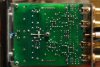
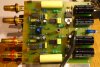
Result : The two IC physically located on "red side" was noticeably hotter than the two IC on "black side" (ref top.jpg).
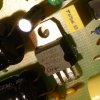
The two device in TO220 cases are 7818 and 7918 voltage regulators (when posting I noticed that not all markings are visible from pictures).
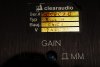
Also, the naming plate for the device is worn out, so even if I have a decent camera and tried to relocate the light source and camera, it's still not all letters that is visible, even for the eyes.
Power supply is 2x25V and measuring the voltage over time I could not detect voltage dropout.
Basically what I ask for help for is
Thanks in advance
I just have got asked to try to repair one RIAA amplifier for a friend.
In this particular case, it works for a while - maybe half a minute, and then the outut is just white noise, both channels.
So I decided to triy to look at it. When first opened, the things that first make my attention was:
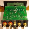
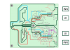
- Device have obvious being opened before and tried to being repaired.
- The four IC have all markings scraped away (This is tha part I need help with) - so I can only speculate. I can always find what is input, output and voltage pins - but maybe not the whole picture.
- There is nota single label that denotes components ID on the PCB.
Result : The two IC physically located on "red side" was noticeably hotter than the two IC on "black side" (ref top.jpg).
The two device in TO220 cases are 7818 and 7918 voltage regulators (when posting I noticed that not all markings are visible from pictures).
Also, the naming plate for the device is worn out, so even if I have a decent camera and tried to relocate the light source and camera, it's still not all letters that is visible, even for the eyes.
Power supply is 2x25V and measuring the voltage over time I could not detect voltage dropout.
Basically what I ask for help for is
- Either if there exist a service manual for this (none found by google)
- Or have the actual name of the IC (opamps or maybe inhouse amplifier IC ?) used here.
Thanks in advance