Continue to Site

Welcome to our site!

Electro Tech is an online community (with over 170,000 members) who enjoy talking about and building electronic circuits, projects and gadgets. To participate you need to register. Registration is free. Click here to register now.

  • Welcome to our site! Electro Tech is an online community (with over 170,000 members) who enjoy talking about and building electronic circuits, projects and gadgets. To participate you need to register. Registration is free. Click here to register now.

Chinese 10V - 50V 60A PWM Electronic Speed Controller with Polarization Reversal Functionality Circuit

Status
Not open for further replies.

Dirk.S

New Member
Hello People,

I'm working on a project and blew some components on the a PWM ESC board. These boards can be found on AliExpress etc.:

https://www.aliexpress.com/wholesale?catId=0&initiative_id=SB_20210911132935&origin=y&SearchText=DC+10V-50V+12/24/36/48V+60A+Motor+Speed+Controller

I created the circuit diagram to understand the function of the circuit to be able to fix it and I thought that I would share it here with you. The circuit has been drawn up in KiCad.
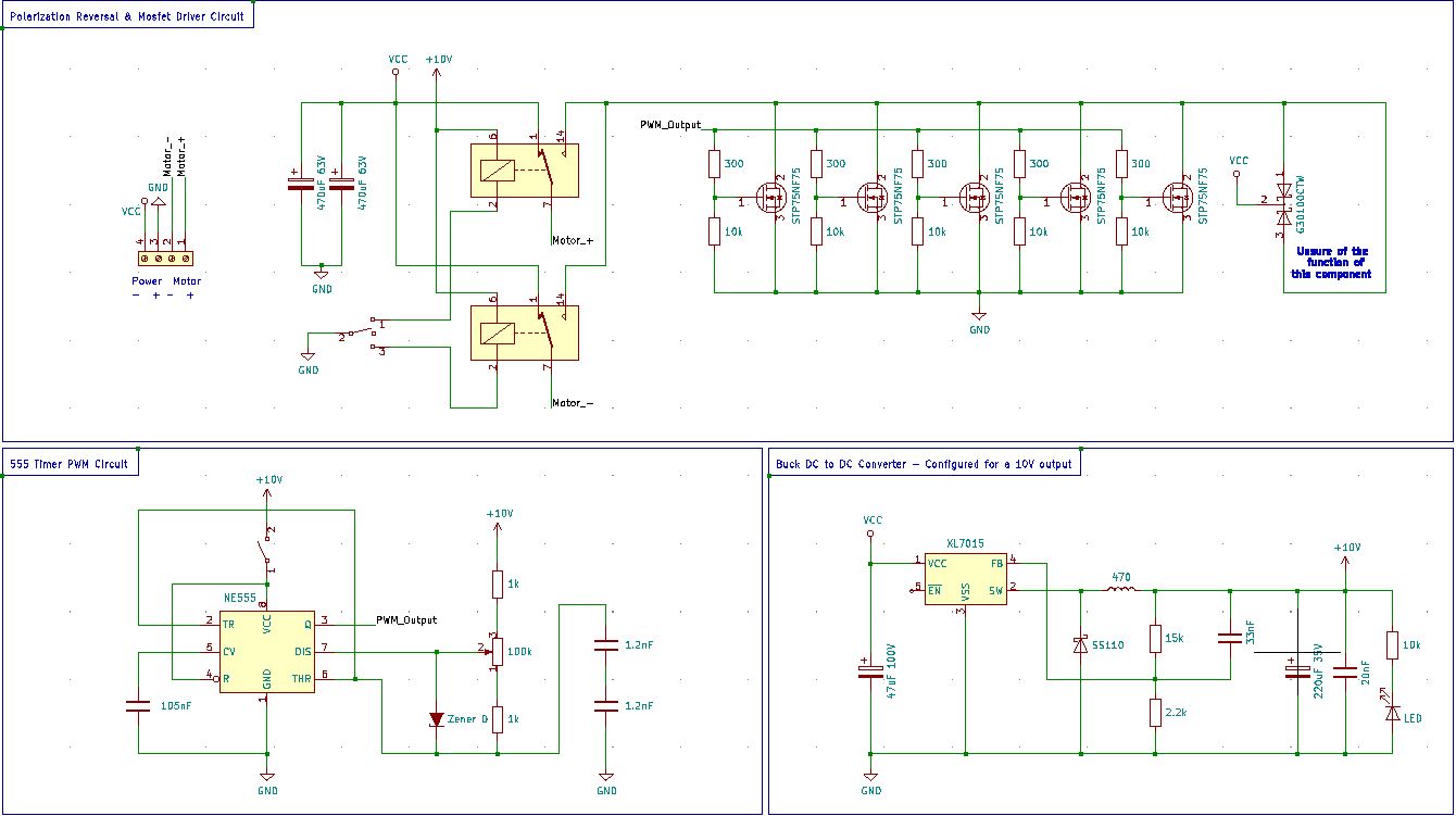
2.JPG


I'm not sure what the function of the Trench Schottky rectifier is in the circuit but I'll leave that for someone to clarify.

Hopefully this helps someone.
 

Attachments

  • ESC_Controller.zip
    5.8 KB · Views: 287
  • Schematic.pdf
    47.1 KB · Views: 361
Last edited:
I'm not sure what the function of the Trench Schottky rectifier is in the circuit but I'll leave that for someone to clarify.

It functions as a "Flywheel diode"; it allows the load current to circulate after the transistors turn off and prevents high voltage spikes that coudl damage the transistors.

The design has an obvious flaw - the gate drive resistors are too high to allow the power FETS to switch quickly; the gate capacitance of those devices is 3.7nF each according to the datasheet, so it takes quite a bit of current to change the gate voltage quickly.

With a 300 Ohm drive resistor the gate capacitance will charge and discharge relatively slowly, causing higher power dissipation in the FETs than if a high current driver were used.
High gate resistiors are not too bad for occasional on-off switching, but at high speeds the inefficiency and power losses could gradually cook the transistors.

The 555 is only rated at 200mA, so could drive 40mA to each device. In high power PWM it's not unusual to have drive circuits capable of 1 - 2A per gate with eg. a 4.7 Ohm or even lower gate drive resistor.

As a compromise, a back-to-back emitter follower driver and going down to eg. 33 Ohm per gate should reduce power dissipation quite a bit?

eg. something like the Q1 & Q2 part of this, added to the 555 output, to boost the current to the FET gate resistors:

nGwou.png
 
Hey there,

Thanks for the feedback, the flywheel arrangement is something that I haven't seen before, thanks for clarifying that (Keep in mind that I'm a newbie when it comes to these things).

I'm not looking at changing the design and building a new PWM ESC at this point in time. I fried the 555 previously and I'm looking at switching the output from the 555 to a PWM output from a micro controller using the following logic level shifter:

2.JPG


Thanks again for the input, much appreciated.
 
OK, you can certainly "level shift", but you still need the high current driver stage between that and the FET gates, or you will just melt them.

That circuit would provide the correct voltage but next to no turn-off current, so the FETs will spend most of their time partly on & dissipating high power levels; the 555 could provide 200mA, that can provide some turn on current but only a fraction of a milliamp turn-off current.

See here for more information:


Look at something like these instead; they can take a logic level input and translate it to a suitable gate drive voltage with 1.5A output current. Each IC has two sections so can drive two FETs. That will give "clean" switching and minimal power loss in the FETs. Use a 6.8 Ohm resistor between each driver output and the FET gate it controls.

Or add that entire driver stage above (from R4 onwards, to R2 driving the FETs, with R4 being R10 in your circuit).
 
It functions as a "Flywheel diode"; it allows the load current to circulate after the transistors turn off and prevents high voltage spikes that coudl damage the transistors.

The design has an obvious flaw - the gate drive resistors are too high to allow the power FETS to switch quickly; the gate capacitance of those devices is 3.7nF each according to the datasheet, so it takes quite a bit of current to change the gate voltage quickly.

I agree with both of those!.

However, the small FET's could be replaced with one n-channel FET to ground, and a pull-up resistor. I've been comparing the NPN/PNP driver circuit with specialised IC drivers, and it seems to work just as well. With just the 555 driving the FET's (even worse with multiple FET's) you'll be wasting a lot of heat in those FET's.

As for his last suggestion, it's obviously a lot better getting rid of the 555 - but still no FET driver, and the FET's will get FAR hotter than they need to. Paralleling the FET's only makes it worse, as it multiplies the already high capacitance.

Here's the driver I'm using from PIC to buck/boost FET - PL2 and Q6 are simply an extra inverter, selectable via PL2 to invert or not - while PWM on most modern PIC's can be set positive or negative, it's best to have the default the correct way to stop killing the FET.

FET_Driver.png
 
Hello There,

Thank you for the info, I had to study up how a MOSFET works again, but I understand now what you meant, thank you for guiding me in the right direction too. I will need to spend some more time on this than what I figured. Thanks again.
 
Status
Not open for further replies.

Latest threads

New Articles From Microcontroller Tips

Back
Top