Continue to Site

Welcome to our site!

Electro Tech is an online community (with over 170,000 members) who enjoy talking about and building electronic circuits, projects and gadgets. To participate you need to register. Registration is free. Click here to register now.

  • Welcome to our site! Electro Tech is an online community (with over 170,000 members) who enjoy talking about and building electronic circuits, projects and gadgets. To participate you need to register. Registration is free. Click here to register now.

Can't interprete this "adaptation circuit"

Status
Not open for further replies.

obr3ptox

New Member
Hello everyone, I'm working on my thesis and came to a point where I can't interprete a part of a circuit I'm using.
This should be an adaptation circuit, so I am guessing it's filtering my signal in some kind of way, but cannot say with certainty which kind of filter should it be.
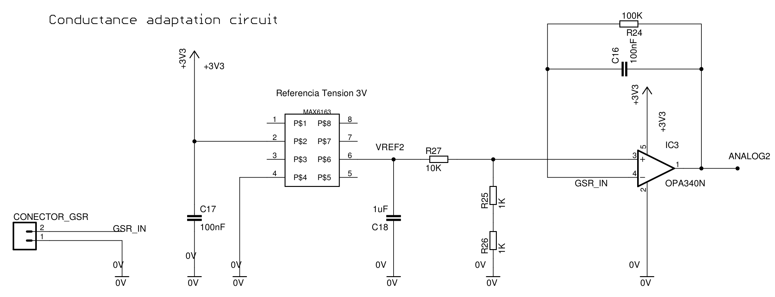
upload_2017-10-23_13-17-46.png

I could say that the most right part is a low pass filter, but then, if I try to think through frequencies, I can't understand nothing more.
Could PLEASE any of you help me?
Thank you, Danke, Grazie <3
upload_2017-10-23_13-17-46.png
 
You have the right method. Break it into pieces. The components around the OPA340N form a filter. The MAX6163 and the 1uF Cap are, per the datasheet, a 3V reference. If you subtract out all of those parts you are left with R27 and R25-R26. What does that look like? A resistor divider. 3V/12k*2k=0.5V. Problem with resistor dividers is there output is dependent on the input impedance of the next stage. Anything within 1 magnitude will have a large effect, 2 magnitude is better, 3 is great. What has an input impedance 3 magnitude more than a 10K resistor divider (talking 1Meg). An opamp. Oh look, an OPA340 is connected to the resistor divider. Not only does the opamp provide filtering, but also isolates the resistor divider from what ever is off the page to the right.
 
Thank you! Well, the page to the right is the whole Arduino path from ANALOG1 input to the ADC :hilarious:
Talking about just the filtering part, am I right guessing it's a low-pass filter? If that, my cutting frequency is calculated through fc=1/2pi*100k*100n ? Assuming that I am right, how could I calculate the voltage gain if I have no other resistors on the OPAMP feedback node?
 
You have the right method. Break it into pieces. The components around the OPA340N form a filter. The MAX6163 and the 1uF Cap are, per the datasheet, a 3V reference. If you subtract out all of those parts you are left with R27 and R25-R26. What does that look like? A resistor divider. 3V/12k*2k=0.5V. Problem with resistor dividers is there output is dependent on the input impedance of the next stage. Anything within 1 magnitude will have a large effect, 2 magnitude is better, 3 is great. What has an input impedance 3 magnitude more than a 10K resistor divider (talking 1Meg). An opamp. Oh look, an OPA340 is connected to the resistor divider. Not only does the opamp provide filtering, but also isolates the resistor divider from what ever is off the page to the right.

Thank you! Well, the page to the right is the whole Arduino path from ANALOG1 input to the ADC :hilarious:
Talking about just the filtering part, am I right guessing it's a low-pass filter? If that, my cutting frequency is calculated through fc=1/2pi*100k*100n ? Assuming that I am right, how could I calculate the voltage gain if I have no other resistors on the OPAMP feedback node?
 
ADWSystems seems to have missed the connection between the input GSR_IN and the opamp, which makes this circuit a little more complicated - it is a current to voltage convertor, with some low pass filtering. With zero input curent the output voltage will be 3V, with input of 30uA the output voltage will be 0V (or close to it).
 
ADWSystems seems to have missed the connection between the input GSR_IN and the opamp, which makes this circuit a little more complicated - it is a current to voltage convertor, with some low pass filtering. With zero input curent the output voltage will be 3V, with input of 30uA the output voltage will be 0V (or close to it).

So, the OPAMP phase is the GSR_IN current convertor, with the low pass filtering operated in the feedback node?
 
What is GSR_IN? Specifically, what is its source or output impedance? Without knowing that, you cannot calculate the gain or the frequency response of the IC3 stage. Note that if the source impedance is 10 K or higher, then the filter does not provide much attenuation.

ak
 
GSR_IN is the value of voltage measured between two electrodes. The only information about the schematics is what I posted in here.
This is part of my bachelor final work, but it is more focused on the bioengineering aspect of the whole subject rather than the electronics part. I was trying to understand this circuit to be ready for any kind of questions the teacher could come up with.
 
Hmm, so in your thesis, that should be written only by you, you present a circuit you know nothing about? Interesting...
 
Hello everyone, I'm working on my thesis and came to a point where I can't interprete a part of a circuit I'm using.
This should be an adaptation circuit, so I am guessing it's filtering my signal in some kind of way, but cannot say with certainty which kind of filter should it be.
View attachment 108804
I could say that the most right part is a low pass filter, but then, if I try to think through frequencies, I can't understand nothing more.
Could PLEASE any of you help me?
Thank you, Danke, Grazie <3View attachment 108804

Hello there,

The op amp part is a low pass filter but only if the GSR source is either a current source or a voltage source with series resistance. A voltage source with series resistance would make sense because then the output could be biased with a known offset.

So with a voltage source and series resistance and calling the feedback resistor R and capacitor C and the input source resistance Rg we have cutoff frequency:
f=1/(2*pi*R*C*K)

where K is:
K=sqrt(R^2+2*Rg*R+Rg^2)/sqrt(R^2+2*Rg*R-Rg^2)

The reason for this is because the input source resistance plays a big part in both the DC gain and the cutoff frequency.

The DC gain from GSR to Vout is simply:
G=-R/Rg

and you see here the resistance Rg must be known or else you can never calculate the output.
 
This is actually not in my thesis. I used this shield for Arduino which is not provided with any kind of datasheet. My objective was to create an interface for the measurement of the GSR, not studying the entire acquisition system. This (Arduino+Shield) had been validated by a colleague of mine, but he left no information about the GSR acquisition schematics.
Since I would like to understand even things that weren't the main focus of the entire job, I was surfing the web for all the schematics and datasheets, but only found this. Which I have difficulties in interpreting since, I just want to remark it, it's just a marginal part not in focus for the whole thesis.
 
Last edited:
Hello there,

The op amp part is a low pass filter but only if the GSR source is either a current source or a voltage source with series resistance. A voltage source with series resistance would make sense because then the output could be biased with a known offset.

So with a voltage source and series resistance and calling the feedback resistor R and capacitor C and the input source resistance Rg we have cutoff frequency:
f=1/(2*pi*R*C*K)

where K is:
K=sqrt(R^2+2*Rg*R+Rg^2)/sqrt(R^2+2*Rg*R-Rg^2)

The reason for this is because the input source resistance plays a big part in both the DC gain and the cutoff frequency.

The DC gain from GSR to Vout is simply:
G=-R/Rg

and you see here the resistance Rg must be known or else you can never calculate the output.

This completely matches my guess. I can clearly see that I miss information about the (what you call) Rg resistance, that's the point where I stuck and looked for help.
Here, having no information about the input resistance (I have been looking for datasheets everywhere but there is none of them) makes it impossible to clearly define frequencies and gain.

Hi,

Yes, and even if it was a current source we would have to know the non ideal resistance in parallel.

If it was a voltage source with Rg=0 then the op amp would not behave like a low pass filter anymore and we could not even calculate the output offset voltage then either. Same if it was a current source with infinite resistance (as a true current source would have) then the op amp still no longer behaves like a low pass filter.
With a true ideal voltage source as input, the output would saturate even with a tiny input like 1mv. Saying that the design depends on unusual characteristics of the op amp is most likely not the answer either because good designs are not done like that especially in instrumentation circuits.

This makes me believe the same as you, that we must find more information. One way is to compare with a known measurement with a known circuit that has been in use already for some time, then compare the responses. We can extract more information that way.

Could it even be that here is a resistor missing on the schematic on the GSR input.
 
Last edited:
Hi,

Yes, and even if it was a current source we would have to know the non ideal resistance in parallel.

If it was a voltage source with Rg=0 then the op amp would not behave like a low pass filter anymore and we could not even calculate the output offset voltage then either. Same if it was a current source with infinite resistance (as a true current source would have) then the op amp still no longer behaves like a low pass filter.
With a true ideal voltage source as input, the output would saturate even with a tiny input like 1mv. Saying that the design depends on unusual characteristics of the op amp is most likely not the answer either because good designs are not done like that especially in instrumentation circuits.

This makes me believe the same as you, that we must find more information. One way is to compare with a known measurement with a known circuit that has been in use already for some time, then compare the responses. We can extract more information that way.

Could it even be that here is a resistor missing on the schematic on the GSR input.

Well...considering they don't provide datasheets (at least, my university claims not to have one), neither they do it on their website, that will be impossible to know. And missing components in the only and unique schematic available on the whole internet, would be quite embarassing.
I assumed values for Rg resistance, just to be sure that this operates filtering high frequencies (which I'm glad it does).
 
upload_2017-10-23_15-48-1.png

Moreover, this is what I just found on the producer's forum... They just don't know what they use in their own product.
 
GSR_IN is the value of voltage measured between two electrodes.
Could the circuit originally have been intended to sense the resistance between two electrodes? I'm thinking GSR = Galvanic Skin Resistance. As others have said, the source resistance/impedance is all-important. This is demonstrated by the following simulation, where resistance is increased from 1k to 100k :-
AdapterGSR.PNG


For these resistance values the filter would benefit from a much higher capacitance value if it is meant to filter out mains frequency.
 
Ignoring the filtering aspect for a moment, the opamp is configured as a Transimpedance Amplifer, also called a "current to voltage converter".

Its application in this case is to measure skin resistance. The circuit is configured to apply a bias voltage across the electrodes. The skin resistance causes a current to flow. The transimpedance amplifer converts the skin current to a voltage at its output.. (Not a linear function).

The voltage reference and divider consisting of R25, R26, R27 applies a 0.500V Bias voltage to the non-inverting input of the amplifier. As long as the opamp is within its linear range, then the negative feedback through R24 will keep the voltage at its inverting input equal to the bias voltage at the non-inverting input. This means that there is a constant voltage of 0.5V applied to the skin electrodes.

Here is a simulation:
2.png


The independent variable of the simulation is Rs, the skin resistance. The log of Rs is plotted along the X axis.

I plot V(in), V(out), and I(Rs) (the current through the skin) as a function of Rs. Note that for values of Rs>~20KΩ, V(in) = V(bias) = 0.500V!

The highest current ever applied to the skin is ~33uA, which somebody considers "safe". The voltage between the skin electrodes never exceeds 0.5V.

Note that the output voltage V(out) is a non-linear function of Rs, and that means that the Arduino code has to implement a "look-up table" or some other means of estimating what the skin resistance is based only on V(out). The "sweet spot" for skin resistance is about 40KΩ, where V(out) changes steeply.
 
Last edited:
Damn, Alec beat me to it, as usual....
 
I added V3 to my sim, which is a "noise" source, and did a frequency sweep.

Capacitor C1 (C16 in your circuit) makes the transimpedance amplifer a single-pole low-pass filter. However, the response is a function of Rs as shown below. The green plot is for Rs=20KΩ, yellow is 40KΩ and so on to violet where R=100KΩ. In other words, the gain is effected by Rs, but the cutoff freq remains constant.
2a.png
I agree with Alec. The low-pass filtering is inadequate to be a proper "anti-aliasing filter" ahead of an ADC.
 
Last edited:
I really appreciated what you two did here. Despite confirming what I lately assumed about this circuit's purpose, both of you gave me hints about the GSR_IN variable.
THANK YOU!
 
Status
Not open for further replies.

Latest threads

New Articles From Microcontroller Tips

Back
Top