Continue to Site

Welcome to our site!

Electro Tech is an online community (with over 170,000 members) who enjoy talking about and building electronic circuits, projects and gadgets. To participate you need to register. Registration is free. Click here to register now.

  • Welcome to our site! Electro Tech is an online community (with over 170,000 members) who enjoy talking about and building electronic circuits, projects and gadgets. To participate you need to register. Registration is free. Click here to register now.

Can someone explain to me how this circuit works (power supply)?

Status
Not open for further replies.

FusionITR

Member
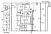
Anybody mind explaining how the auxiliary winding of this power supply is suppose to work? I have never seen this design for a auxiliary power supply before in other SMPSs I have done.

I understand the switching current in the secondary will switch with the switching of the primary, but I don't understand the current paths of the secondary, what role the cap plays (DC isolation for the ZCD?) or the non-zener diode.
 

Attachments

  • aux2.png
    aux2.png
    58.1 KB · Views: 246
Last edited:
This is a power factor corrector. I think you want a boost converter. I will not talk about PFC and go to the boost converter part.

F1 fuse.
C1,2,3,4, LF1 noise filter
NTC is a inrush limiter.
BD converts AC to DC.
C5 main input filter. DC at this point.

Q1 when on causes current to flow through T1 to ground. T1 being an inductor not a transformer. (At this point.) Then Q1 opens up the current flowing wants to keep flowing. The voltage at T1-Q1d flys up to more than the DC on C5. The current goes through D2 into C9. When the current runs down (or when Q1 turns on) the foltage on Q1d drops back. The point of this thing is to make VC9 greator than VC5.

T1 has a secondary that sends power to the "FAN7529" and sends a signal into pins 3 and 5,6.

R10,11 is for feedback. In a PFC the out put voltage is 400 volts.

What do you want to know?
 
I know how the rest of the circuit works, I've done SMPS power supplies before, I was specifically asking about the auxiliary power supply (second winding of the transformer powering the chip after startup).
 
Sorry, I just reread my OP, I didn't word it right, i see how you were confused.

Edit: edited the OP
 
Last edited:
R3 (470k) slowly charges up C6 to get thinks started.
When running the AUX. power comes from T1.
R4 (10 ohms) softens the edges.
The voltage on T1 is complex.
In a PFC the input "DC" is not really DC it is half sign waves. (full wave)
If the input is 110vac then the voltage at C5 is in the range of 0 to 160 volts.
120 1/2 sign waves / second.

When the FET is on the voltage cross T1 is someware in the range of 0 to 160 volts depending on the power line voltage at that time.

When the FET is off the voltage is 400-input voltage.

(if this was a boost supply the voltage on T1 would be simple. Vin and Vout-Vin.)

The P to P voltage on T1 is simply 400 volts. via turns ration the secondary is about 15 volts peak to peak. Centered around 0 volts.

C10 AC couples the signal.
ZD1 clamps the signal to ground. (-0.7 volts)
Now the the signal is from 0 to 15 volts.
D1 peak rectify the siganl and not C6=15 volts.

Now it does not matter if the power line is at near 0, or 50 volts or 100 volts or 150 volts, C6 is about 15 volts.

questions???
 
Sorry but I have further questions.

Internal to the FAN7529, there is a 22V clamp, so I understand that R3 charges to ~18V the clamps at that voltage to start up the IC.

Then the IC starts up the switching cycles to T1 which appear at the secondary at whatever turns ratio your transformer happens to be. The AC part of the secondary couples through C10, but because of the 18V ZD1 clamp D1 is reverse biased, therefore the voltage at ZD1 should bounce between Vsec and 18V

Thats where I am confused at, how is the voltage at ZD1 powering the IC when D1 is reserve biased?
 
ZD1; Change to a normal diode! Think of R4=0, C10=large

C10, ZD1, D1 make a recrifier that will cause the voltage on C6 = the peak to peak voltage comming from T1 secondary.

------------------------------------
for this example only; the voltage from T1 secondary is square wave +7 volts and -7 volts. The average is 0 volts!
C10 removes the "average = 0 volts"
ZD1 causes the -7volts to clamp at -0.7 volts. The p-p is 14 volts so the positive is 13.3 volts. On the positive half the 13.3 volts flows through D1 to make 12.5 volts on C6.
------------------------------------
disclamer, not 50%, not +/-7 volts, not 12.5 volts (example only)
 
ZD1 is an 18V zener. It will not make a rectified voltage since the output at ZD1 will clamp at 18V and the vcc clamps at 22V (according to the datasheet).

If a +/- 7V square was is coming out of the secondary of T1, I agree, the zener will see +/-7 which will get clamped at -0.7V, how do you get 13.3Vpp? It would be +7 + 0.7 = 7.7Vpp. To get a 0.7V drop and there would have across D1 there would have to be a positve flow of current but D1 is reverse biased

Accord to the datasheet, vcc will clamp at 22V when charged through R3. 22V at once side of the D1 and 18V (assuming ZD1 clamps on the positive side). D1 is reverse biased and no current flows through it.
 
>You are thinking too much.
>The 22V clamp should never happen! This is only to protect the IC. As soon as the IC starts to work it will pull much more power than can come from R3 and the voltage on C6 will start down fast. I have made many PFCs and have never seen the clamp voltage happen.
>It is unlickly the zener will turn on in zener mode. (It will not have 18 volts across it, or not fore more than a uS.
>The transformere will ring! R4 and ZD1 will clamp the ring. This is not the main body of the wave form. Thinking about 18V is part of the problem.
>If there is a +/-7V signal, and the -7V is clamped at -0.7V then the positive voltage is 14-0.7=13.3 (check my math)
>if the most positive signal part is 13.3 then D1 eats up another 0.7 then 13.3-0.7=12.6.
>Even if my math is strange....This is a cap/two diode rectifier. Output=(input p-p) - two diodes. 14-1.4=12.6
 
So in summary--

1. IC will start long before internal clamp
2. ZD1 zener clamp is irrelevant since IC will be powered from the secondary of T1 before V(zd1) clamps at 18V
3. What is Vaverage at the vcc pins of the IC when vcc is powered from T1 secondary?
 
The IC starts at 12V (+/-1v). Stops at 8.5V (+/-1v). It will run happily about anywhere. Stay away form 22v because the part heats up. The internal Zener gets hot. Stay away from 8.5 because the part might shut down. This depends on what FET you have. 10V to 12v is good for many FETs. Some old parts like 15v gate drive.

This part is at end of life! Do not use on a new design. It is fine for a home project.
 
The reason why I ask is because it doesn't seem like based on theoretical circuit design you can just look at it and determine what the operating point of the IC will be.

Why is this part at the end of it's life? I actually plan on rolling a product out based on this IC.
 
The reason why I ask is because it doesn't seem like based on theoretical circuit design you can just look at it and determine what the operating point of the IC will be.

Why is this part at the end of it's life? I actually plan on rolling a product out based on this IC.

https://www.fairchildsemi.com/pf/FA/FAN7529.html "life time buy"
There are many PFC parts on the market. Much of the theory is the same.
Are you suing this for power factor correction?
 
Life time buy means that in the next X months you must place orders for all the parts you will ever need. They will no longer make the part.
 
BTW, while we are on the subject, do you know of any suppliers that have premade triple output flyback transformers? I have found a few but they are very low current. Looking for one that has high power secondaries.
 
Digikey has 26,966 in stock, I don't think I will have to worry.
When those are gone, that is it! Maybe if you only make 1000 then OK. I can eat that many in a month.
If you have plans to produce long turm then..........
 
Status
Not open for further replies.

Latest threads

New Articles From Microcontroller Tips

Back
Top