PG1995
Active Member
Hi,
I've always understood that for an NMOS the drain should be at higher potential compared to the source; in other words, Vdd should be connected to the drain terminal and source terminal should be grounded for proper function. Vgs should be greater than or equal to Vtn
In case of PMOS, the source terminal should be at higher potential compared to the source, and Vgs should be less than or equal to Vtp, or Vsg should be equal to or greater than Vtp.

Source: https://www.digikey.com/en/articles/the-significance-of-the-intrinsic-body-diodes-inside-mosfets
So, the body diode lets the current flow from source to drain without any channel in case of an NMOS.
The body diode is a result of connecting body terminal to source terminal internally in discrete NMOS transistors. I'm emphasizing on "Discrete NMOS" because many weblinks seem to emphasize this point as well; check Link 1 and Link 2.
Link 1: https://electronics.stackexchange.com/a/389409/246366
Link 2: https://electronics.stackexchange.com/a/105561/246366

Source: https://electronics.stackexchange.c...tand-the-intrinsic-body-diode-inside-a-mosfet
Question 1:
So, in case of discrete NMOS, the body terminal is connected to source terminal but what about integrated circuits? I think in ICs body terminal would be connected to circuit's ground rather to the source of any transistor? For PMOS, the body terminal would be directly connected to the main power line, i.e., Vdd. Could you please confirm this?
Question 2:
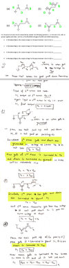
The capture below has been taken from the attachment titled "Pass_1, https://www.electro-tech-online.com...136257/?hash=853c71bf3277105a2fdd29712da93eef . The answers provided are correct but I don't understand the connections. I labelled the connections as "Drain" and "Source" myself. In the attachment they also use the same kind labelling and also on some other webpages I found the same scheme of labelling. think these circuits are classified as pass transistors. For example, look at image part "(d)" below. The drain of PMOS is at higher potential compared to the source, and the source of NMOS is at higher potential compared to the drain. I don't know how such circuits are working in reverse manner where drain and source terminals have been reversed. Does it have something to do with body terminal? Could you please help me?

I've always understood that for an NMOS the drain should be at higher potential compared to the source; in other words, Vdd should be connected to the drain terminal and source terminal should be grounded for proper function. Vgs should be greater than or equal to Vtn
In case of PMOS, the source terminal should be at higher potential compared to the source, and Vgs should be less than or equal to Vtp, or Vsg should be equal to or greater than Vtp.
Source: https://www.digikey.com/en/articles/the-significance-of-the-intrinsic-body-diodes-inside-mosfets
Source: https://www.digikey.com/en/articles/the-significance-of-the-intrinsic-body-diodes-inside-mosfetsCurrent typically flows from the drain to the source in N-channel FET applications because of the body diode polarity. Even if a channel has not been induced, current can still flow from the source to the drain via the shorted source to body connection and the body to drain diode. Because of this, a typical N-channel FET cannot block current flow from its source to its drain.
So, the body diode lets the current flow from source to drain without any channel in case of an NMOS.
The body diode is a result of connecting body terminal to source terminal internally in discrete NMOS transistors. I'm emphasizing on "Discrete NMOS" because many weblinks seem to emphasize this point as well; check Link 1 and Link 2.
Link 1: https://electronics.stackexchange.com/a/389409/246366
Link 2: https://electronics.stackexchange.com/a/105561/246366
Source: https://electronics.stackexchange.c...tand-the-intrinsic-body-diode-inside-a-mosfet
Question 1:
So, in case of discrete NMOS, the body terminal is connected to source terminal but what about integrated circuits? I think in ICs body terminal would be connected to circuit's ground rather to the source of any transistor? For PMOS, the body terminal would be directly connected to the main power line, i.e., Vdd. Could you please confirm this?
Question 2:
The capture below has been taken from the attachment titled "Pass_1, https://www.electro-tech-online.com...136257/?hash=853c71bf3277105a2fdd29712da93eef . The answers provided are correct but I don't understand the connections. I labelled the connections as "Drain" and "Source" myself. In the attachment they also use the same kind labelling and also on some other webpages I found the same scheme of labelling. think these circuits are classified as pass transistors. For example, look at image part "(d)" below. The drain of PMOS is at higher potential compared to the source, and the source of NMOS is at higher potential compared to the drain. I don't know how such circuits are working in reverse manner where drain and source terminals have been reversed. Does it have something to do with body terminal? Could you please help me?