Continue to Site

Welcome to our site!

Electro Tech is an online community (with over 170,000 members) who enjoy talking about and building electronic circuits, projects and gadgets. To participate you need to register. Registration is free. Click here to register now.

  • Welcome to our site! Electro Tech is an online community (with over 170,000 members) who enjoy talking about and building electronic circuits, projects and gadgets. To participate you need to register. Registration is free. Click here to register now.

alternating tone using a 555 timer

Status
Not open for further replies.

meowth08

Member
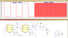
We were asked to design an alternating tone using a 555 timer. One tone is 450Hz that lasts for 90 seconds and the other tone is 15kHz that lasts for 60 seconds. Actually, I've already started with the design patterning it to the "burglar alarm system" schematic Sir Eric provided last time. In this design, I used 2 monostable to produce the 90 seconds and 60 seconds time requirements. Each monostable is connected to an astable circuit. Each astable circuit was made to oscillate at the required frequencies with these following assumptions:

first astable: 450Hz
frequency=1.44/[(R1+2R2)C]
duty cycle=R2/(R1+R2)

I'm not sure if the equation for duty cycle is correct. I've also read some articles that computes duty cycle as R2/(R1+2R2). which is which???

second astable: 15kHz
frequency=1.44[(R1+2R2)C]
duty cycle=R2/(R1+R2)

Since what is desired is that the tones alternately sound, I used a total of (90sec+60sec)=150 sec to finish 1 sequence (i.e. 450Hz then 15kHz). Dividing 90 by 150, I got a duty cycle for the 450 Hz tone as 0.6 while 60/150 yields 0.4 duty cycle for the 15kHz tone.

Giving a value for C for the astable, and substituting values, R1 and R2 were readily computed.

My problem is that I do not know exactly what to do next. I am thinking of delaying the first tone for 90 seconds. But how would I do that? After 90 seconds, the 15kHz will prevail. Then after 60 seconds, the 450 Hz again which will continuously alternate.

To achieve the alternation I was also thinking to connect the outputs of the the two astables to a 2to1 demultiplexer, if there is such, then to an amplifier. :)

If there are mistakes in my design or if the design is a total mistake, please educate me my learned friends. Many thanks in advance.
 
Last edited:
hi,
For the Astable Ver 1, the Freq = 1.44/[(R1+ 2*R2)]*C)
Where the resistors, R1 is from the +Vs to pin7 and R2 is between pin 7 and 2&6, Cap from pins 2&6 to 0V.

For Astable Ver 2, where the output pin 3 is connected back via R1 to pins 2&6, Cap from pins2&6 to 0V. Pin 7 is n/c.
Note: Astable V2 gives close to a 50/50 mark space ratio on pin3. Also a second output can be taken from pin 7, requires a 10K pull up to +Vs.
The Freq = 1/[1.4*(R1)*C]

Look at this image for one option.
 

Attachments

  • TwoTone1.png
    TwoTone1.png
    24.6 KB · Views: 305
Last edited:
Thank you again Sir. I think I'll have to read more articles about the 555 timer before I understand the design. I still have to study the internal circuitry of this IC so I could trace the signal from input to output. I think this 555 timer is really amazing. Basically, it functions as monostable (a one shot pulse generator) and astable(an oscillator ), but it surprises me always. Proper connections with proper component values could yield different output with different periods and frequencies. Another exciting thing about this is that this IC was used in a competition in this site. :)
 
Last edited:
Hello sir,

Kindly verify my explanation on the schematic.

The output of U1 controls Q1. U1 is high for 90.68444563 sec. This is the time the capacitor charges. Then the capacitor discharges through the 580k resistor for 59.09772861 sec. For 90 sec, collector-emitter of Q1 acts as open. Therefore the 10n capacitor charges for 1.102104017 milliseconds and discharges through the 159k resistor. The total time of charging and discharging is 2.204208034 milliseconds. This yields a frequency of 453.6776858 Hz. This frequency will hold as long as (o1) is high. After 90.68444563 sec, (o1) will be low. That makes collector-emitter of Q1 act as short. This time, the 10n capacitor charges and discharges through the 4.7k resistor for 65.15583497 microseconds which yields a frequency of 15347.81958 Hz.

With these values of frequency, I now realize the importance of using a resistor in series with a variable resistor. That would make tuning easier. Using a potentiometer would really require coarse adjustments. :D I hope D8 will also go through the schematic and read this post. Maybe, he'll be convinced afterward.

And yes, I already understand that the mark space ratio on (o2) is 50/50. But you said close to 50/50 because of the presence of the 10n capacitor connected between pin 5 and ground. This capacitor would vary the duration of the waveform as stated in the datasheet of TLC555. Pin 7 of U1 is used as an auxiliary output. Since the output on pin 7 is low when the output on pin 3 is high, a pull up resistor of 10k is needed. Actually sir, I don't know why the value of the pull up resistor is 10k. Well, it's the operation of the circuit that's important to me this time. Maybe, I'll be able to know why 10k is used through my readings later.

I wish I can also use LT-SPICE and learn how to simulate using the program. I downloaded the application but when I clicked on the "run" button, a message was displayed saying that "This is not a valid win32 application.......". :p
 
Last edited:
That makes collector-emitter of Q1 act as short. This time, the 10n capacitor charges and discharges through the 4.7k resistor for 65.15583497 microseconds which yields a frequency of 15347.81958 Hz.

hi m8,
A small point to consider is that the 159K is in parallel with the 4k7 when the transistor is switched ON. If you ignore the ON 'resistance' of the transistor, the total value is ~4k6.

The pin 7 output, as we discussed in Chat is an open collector output, so an external pull up resistor is required if the pin is used. I chose 10K , because the of the transistor on pin 7 is connected as an emitter follower, so the Base current required is quite low in this application.

The datasheet gives the maximum sink current for pin7, so you would choose a PU resistor that limits the current to that maximum value.
 
Oh yes! I committed a mistake on that part Sir.

Regarding PU, is this the same concept to that of the additional resistors you added in my line follower project?
 
Oh yes! I committed a mistake on that part Sir.

Regarding PU, is this the same concept to that of the additional resistors you added in my line follower project?

hi m8,
The resistor in the line follower was to sink leakage current and avoid it flowing into the transistor Base.
 
Status
Not open for further replies.

Latest threads

New Articles From Microcontroller Tips

Back
Top