Continue to Site

Welcome to our site!

Electro Tech is an online community (with over 170,000 members) who enjoy talking about and building electronic circuits, projects and gadgets. To participate you need to register. Registration is free. Click here to register now.

  • Welcome to our site! Electro Tech is an online community (with over 170,000 members) who enjoy talking about and building electronic circuits, projects and gadgets. To participate you need to register. Registration is free. Click here to register now.

Allocating registers from RAM for own use

Status
Not open for further replies.

Peet19

Member
Hi!
I want to allocate registers from RAM for my own use using CBLOCK. So far, I’ve started booking from address 0h, but the interrupt is at address 08h. This is not a problem? Can only 7 bytes of registers be reserved?
Vagy 0x20-kor kezdjem?
CBLOCK 0
CNT1
CNT2
ENDC
 
You just need to look at the User Manual for that chip to see the vast amount of Ram available on that chip.
As you are using Assembler its an invaluable manual.

Also have a look at the Templates folder which gives the basics of how to set up the code.

Typical examples of similar chips below, though yours many be slightly different so do download the manaul for your chip.


001197.jpg
001199.jpg
 
As I said above, GPR's (RAM) are completely separate in Harvard devices - they are not related at all.
Historically PIC's used banks of memory, in this device it's 'optional' - but you can configure it as you wish. Then the bottom bank (bank 0) can become a mix of GPR's and the SFR's (actually in bank 15), making SFR access quick and easy. Or you can use the BSR to access the full range of GPR's, with the SFR's up in bank 15.
 
Do not fully understand.
I booked 0xFD6 which is the address of TMR0 and then I could easily overwrite it.
Code:
CBLOCK    0XFD6
    CNT1
ENDC

DECFSZ CNT1
 
Do not fully understand.
I booked 0xFD6 which is the address of TMR0 and then I could easily overwrite it.
Code:
CBLOCK    0XFD6
    CNT1
ENDC

DECFSZ CNT1

TMR0 is an SFR, so not in program space - so obviously can be written to and read just as GPR's can.

But why would you deliberately be over writing SFR's?.

Perhaps you should study the memory organisation chapter in the datasheet?.
 
I ask because I don’t want to accidentally overwrite any SFR.
In the picture I see that the program memory is up to 3FFFh and the GPR starts from 4000h?
Where can it be used the memory?
Képernyőkép 2022-06-09 20-32-04.png
 
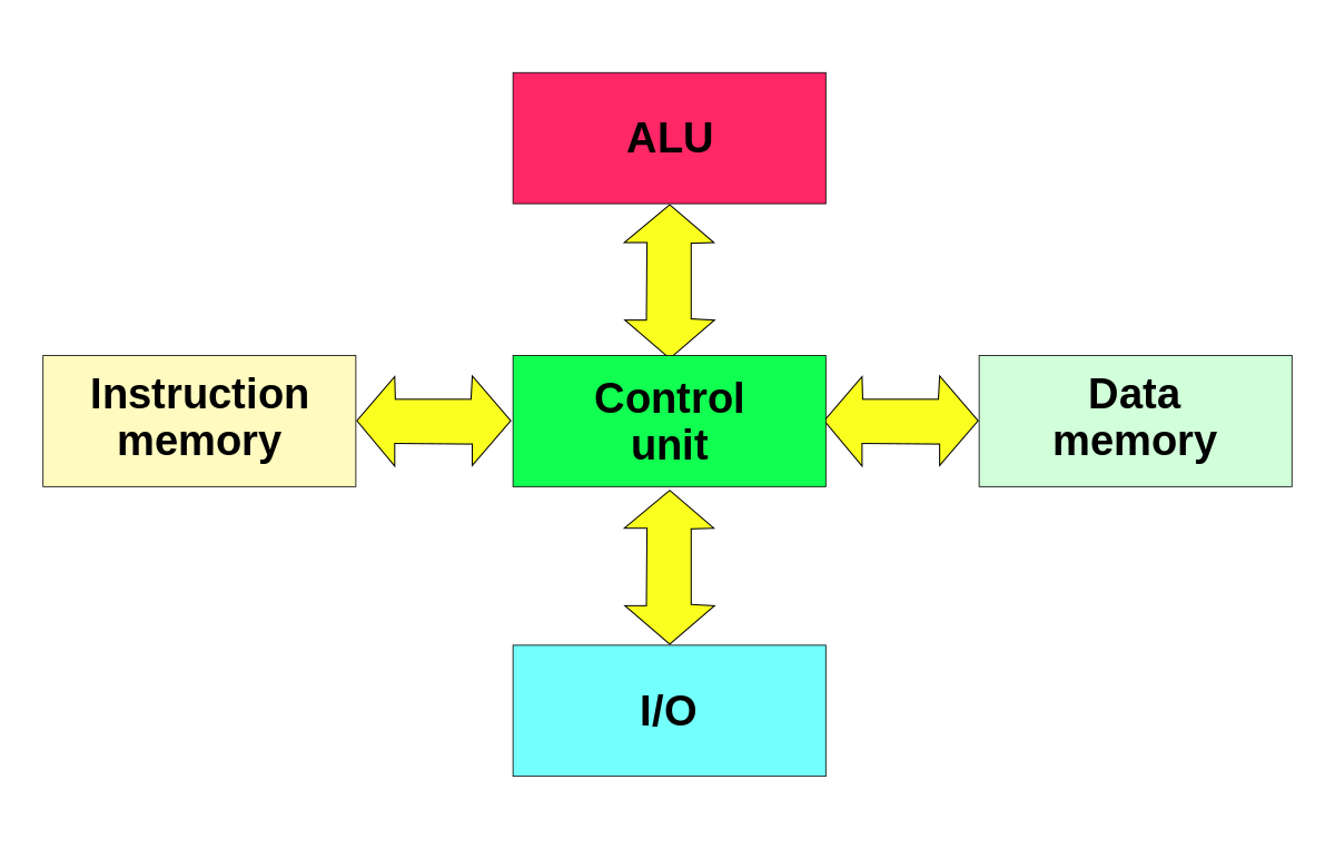
Program memory and Data memory (RAM / registers etc.) are two totally separate areas with their own independent address maps.

Instructions that read or write RAM or registers etc. cannot access the program part, and the program instructions (code) is never read from the registers/RAM.
(It needs special indirect instructions to read data from program space, it cannot be done directly).

That's the "Harvard architecture" Nigel mentioned; very different from many other CPUs that treat program and data space the same.

 
Yes, I understand that now, thank you.
The program memory is 16 bits and the data memory is 8 bits and the two are completely separate.
In the file register 000h-2FF is the data memory 768 bytes. From 300h in turn restricted. What does that mean?
 
You have chosen a quiet advanced chip to start your program learning.
Is there any way you could use a more basic chip from the Pic16F range like a pic16F877A / 76A etc ?

For the Pic18 the Ram area can be quiet confusing.

From the picture below you can see that you have two "banks" of Ram , Bank 0 or Bank 1, other similar chips may have many more Banks like 2 -8 etc.

To use Bank1 or above you need specify in your code that you want to use a particular Bank with the BSR.

However for Bank 0 you do not, its contents are always available to the system regardless of what other Bank you may be using, thats why Bank 0 is called the Access bank.

To confuse matters, the system needs some Ram for its Registers and they reside in part of both Bank 0 and Bank15, as shows in the pic below, and you must not use those areas in your code,

Where is says" Unused, Read as 00" , simply means there to is no Ram there to use.


Code:
    cblock 0x00              ;  Bank 0   Access Ram      Use  0x00 to 0x5F Only
    d1,d2,d3,d4                        ; delay work files

    PORTAOLD                        ; main loop files
    PORTACHG
    PORTEOLD
    PORTECHG
    FIRES
    RECOVER

    endc


    cblock    0x100            ; Bank 1

    endc

001200.jpg
 
You have chosen a quiet advanced chip to start your program learning.
Is there any way you could use a more basic chip from the Pic16F range like a pic16F877A / 76A etc ?

I would agree, it's a complicated device to start on - and it doesn't help that pretty well all the assembler tutorials out there are for the far easier 16F series.

I mainly use 18F devices these days, but use XC8 rather than assembler - I've never had any reason to use assembler on an 18F.
 
Hi!
Now I understand the memory map. I still have so many questions that there are symbolic names next to the titles at the beginning of the file register. What does that mean?
I chose this PIC because there is a lot of it out there.

kp.png
 
The assembly language is very sympathetic to me. I also programmed in C but the assembly is much more interesting. Although I'm still in trouble with math operations.
 
Hi!
Now I understand the memory map. I still have so many questions that there are symbolic names next to the titles at the beginning of the file register. What does that mean?
I chose this PIC because there is a lot of it out there.

View attachment 137426
You need to read the datasheet - it's all explained in there.

For a clue, many of those are bits in ADCON2.
 
Status
Not open for further replies.

Latest threads

New Articles From Microcontroller Tips

Back
Top