Continue to Site

Welcome to our site!

Electro Tech is an online community (with over 170,000 members) who enjoy talking about and building electronic circuits, projects and gadgets. To participate you need to register. Registration is free. Click here to register now.

  • Welcome to our site! Electro Tech is an online community (with over 170,000 members) who enjoy talking about and building electronic circuits, projects and gadgets. To participate you need to register. Registration is free. Click here to register now.

A good PCB layout for Dual Active Bridge

Status
Not open for further replies.
Hello people!
I am working on Dual Active Bridge with following specifications:
  1. Frequency=50KHz
  2. Input Current 20A(rms)
  3. Input Voltage=60V
  4. Output Voltage 400V
  5. Output Power=1.2KW
The schematic looks somewhat like this :
IMG_20190215_013836.jpg

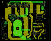
The inductance in blue is the discrete inductance I will add separately apart from that of leakage of transformer, However I want to eliminate the Inductances marked in red. Before starting the layout I wanted some tips from you guys. Also, I would be really obliged if someone can guide me to some reference materials.
One more thing I want to mention is that I have to make a generic layout which will also have provision of paralling of FETs. Like instead of Q1 I will add two FETs Q1a and Q1b and similarly for all switches.
 
If you are paralleling MOSFETs (even if you aren't), lay out gate resistors as close as possible to the gate to protect against ringing and such.

You seem to be missing flyback diodes unless you plan on relying on the parasitic body diode of the MOSFETs (not a good idea IMO). You might want to make room for R-C snubbers as well...just in case. Best location would probably directly across the largest coil inductances though you could place one in parallel with each MOSFET.

Keep the loops small, for both the power MOSFETs and the gate drive.

I think for 20A you will need to use two or more parallel MOSFETs anyways.

400V? Pay attention to PCB clearances/creepage distances. There are multiple standards:
Example 1:
https://www.smpspowersupply.com/ipc2221pcbclearance.html

Example 2:

1550190153029.png
 
Last edited:
I think you want to warry about impedance which inductance is part of.
Keep wire length short and wide. Put small high frequency capacitors close to the MOSFETs.
On the output side make the 4xdiodes+transformer+ceramic capacitor loop small. You then can have a little distance to the Co.
On the input side, same thing. The Ele. Cap. is not good at high frequencies and it will take some distance to connect to it. So have a small cap right at the MOSFETs.
1550197337641.png

The MOSFETs will heat the board and surrounding components. Ele. Caps. do not like to run hot.
50khz is not really that fast but …. the switching edges are fast and you do not want an antenna in the PCB traces. (keep the current loops small)
 
Here is how I placed and routed my fullbridge. Two branches with two bulk caps each, then a pair of film impulse caps as close as possible to the igbt pairs.
It is going to be a welder so there are isolation slots everywhere, but I hid them for better clarity. Since it is a one-off I am using copper wire soldered along the traces to get adequate crossection.
 

Attachments

  • powerboard.PNG
    powerboard.PNG
    71.5 KB · Views: 209
Post #1 shows inductance in between MOSFETs and large caps. You do not want that inductor(s). Can not move the large caps to the transistors, so put small caps at the transistors.

Large caps have inductance inside.
 
Status
Not open for further replies.

Latest threads

New Articles From Microcontroller Tips

Back
Top