Continue to Site

Welcome to our site!

Electro Tech is an online community (with over 170,000 members) who enjoy talking about and building electronic circuits, projects and gadgets. To participate you need to register. Registration is free. Click here to register now.

  • Welcome to our site! Electro Tech is an online community (with over 170,000 members) who enjoy talking about and building electronic circuits, projects and gadgets. To participate you need to register. Registration is free. Click here to register now.

4013 ic test cicuit

Status
Not open for further replies.

neptune

Member
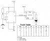
i created my own test circuit for 4013 ic.
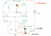
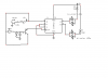
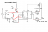
what i have done is use of voltage devider circuit. it devides 9v battery to 3.5v and 1.5 v which are required Vih logic'1' & Vil logic'0'.
for output i have connected pnp transistor because Ioh= -1.36ma. so connected to base which will drive led. i left open other pins.
i have not tested this circuit yet but i want u guys to tell me if this circuit will work or not.
 

Attachments

  • d latch.jpg
    d latch.jpg
    32 KB · Views: 1,774
Are your values absolute max/min ratings? ( I'm too lazy to look them up ) A simple switch will not work for the clock input. At a minimum, you need a "debounce" circuit. Your indicator circuit will light when your DUT is in reset. Q=LOW. Also, your divide resistors don't produce the voltage you want.
 
Last edited:
they are absolute maximum ratings.
"Your indicator circuit will light when your DUT is in reset. Q=LOW." why is that. should i connect npn transistor up there.
and whats wrong with voltage devider circuit is that the value of resistor ?
 
circuit does not work

just for fun I put your circuit into Tina
attached are results.
you never achieve a LOW for data input
your switch won't clock properly as it will bounce
just use a 555 clocking very slow to see how the 4013 works
attach LEDs to the outputs and data in to see what states the pins are
 

Attachments

  • gate circuit.PNG
    gate circuit.PNG
    33.8 KB · Views: 1,476
Your 4013 is not powered so it won't work.
Its output current depends on its supply voltage.

Its input voltages of +3.5V high and +1.5V low are only when its supply voltage is +5.0V, not when it is +9V.

Your +3.5V and +1.5V settings will be reduced as your 9V battery runs down and should be powered from a regulated voltage. A low dropout 5V regulator should be used.
 
"Your indicator circuit will light when your DUT is in reset. Q=LOW." why is that. should i connect npn transistor up there.
and whats wrong with voltage devider circuit is that the value of resistor ?


You definitely need to reconfigure your transistor. I was confused originally by the lable "9V" on the ground side of the battery. I think other's have answered some of your questions.
 
Last edited:
here is a test circuit

for the 4013
plain n simple
should work??
 

Attachments

  • d flipflop.PNG
    d flipflop.PNG
    20.6 KB · Views: 2,313
I think your transistor need some kind of bias on the Emitter. I wouldn't trust the circuit as shown.
 
Laurier also got it wrong.
You must never let a Cmos input float. It needs a resistor to ground for it to be low.

Your High-Low switch does nothing because your D input is connected to +9V.
 
only got half wrong??

the high low switch is correct I am pretty sure
the 9v is connected to D input for high
when switched to low the resistor R3 is grounded.
I might should have R3 connected to 9v then ground w/ switch??
revised schematic. Probably have too many resistors connected to transistor.
attempt to keep current low I guess??
started inputting into Tina to experiment w/ different configurations.
not right I am pretty sure but ??
 

Attachments

  • d flip flop2.PNG
    d flip flop2.PNG
    26.3 KB · Views: 1,870
Naw, the hi/lo switch won't work. The D input should be connected between the resistor and switch. Look at how you have the clock connected to R2. That's how it should be done ( think of the transistor as analogous to the switch ).

And R3 is going to prevent the clk signal from getting to a reasonable low. By R3, I mean the 10K on in the emitter, not the 1K one in the base circuit.
 
Last edited:
It is simple to wire the switch to be high-low and to wire the transistor to pull-up and the resistor to pull-down the CLK pin.
 

Attachments

  • CD4013 circuit.PNG
    CD4013 circuit.PNG
    17.6 KB · Views: 11,706
if i use +5v as a souce. and if i use flip flop multivibrator as a input to clock. will my circuit work ?

i have understood all of the thing above.
but how u people are using clock circuit. whats the role of capacitor connected to base of transistor ?
 
if i use +5v as a souce. and if i use flip flop multivibrator as a input to clock. will my circuit work ?

That would be ideal. A 555 circuit will work. Since the 4013 is a CMOS device, 9V is okay.

i have understood all of the thing above.
but how u people are using clock circuit. whats the role of capacitor connected to base of transistor ?

The resistor and capacitor together make what is known as a RC timing circuit. During the time it takes for the cap to charge, the mechanical vibrations of a switch are ignored, resulting in a clean signal to the base of the transistor.
 

Attachments

  • 4013help.JPG
    4013help.JPG
    26.4 KB · Views: 879
Last edited:
Data shouldn't float ??

I revised so data isn't floating. I assume it shouldn't.
 

Attachments

  • d flip flop2.PNG
    d flip flop2.PNG
    28.6 KB · Views: 595
You do not need the 10k resistor at the D input of the CD4013. The switch should be wired so it connects the D input to either +9V for a logic high or to 0V for a logic low.
 
I'd probably leave it the way it is. Either way works. The resistor insures that the input never floats.
 
http://C:\Documents and Settings\intex dem\Desktop

i have only pnp transistor available to me. i think i can reverse all polarity and use it in circuit.
this shall not create any problem
 
Last edited:
i am new to ic working so please help.
in 4013 datasheet it is given that Ioh= -1.3mA if conditions Vdd=10V, Vo=9.5V .
and Iol = 1.3mA if conditions Vdd=10V, Vo=0.5V

why you all have connected q output directly to +9v through 330 resistor. will not +9v battery push Iol(1.3ma) back current when q is low.
rest of the circuit is understandable.
 
Status
Not open for further replies.

Latest threads

New Articles From Microcontroller Tips

Back
Top