Continue to Site

Welcome to our site!

Electro Tech is an online community (with over 170,000 members) who enjoy talking about and building electronic circuits, projects and gadgets. To participate you need to register. Registration is free. Click here to register now.

  • Welcome to our site! Electro Tech is an online community (with over 170,000 members) who enjoy talking about and building electronic circuits, projects and gadgets. To participate you need to register. Registration is free. Click here to register now.

4 input XOR gate

Status
Not open for further replies.

fingers

New Member
Hi,

Can anyone tell me a part number for a four input XOR gate - I can't find one. eg 74HC..
 
Wow hard one. You may have to make it.
Here are my search results

four input XOR gate
four input exclusive or
4-input XOR gate
4-input exclusive or
xor4
**broken link removed**

**broken link removed**

**broken link removed**

1134H 4-Input Exclusive-OR-Function Logic Gate General Micro-electronics Inc
http://www.americanmicrosemi.com/catalog/1134H.html

2134H 4-Input Exclusive-OR-Function Logic Gate General Micro-electronics Inc

PAL20X10a Programable Logic IC
http://www.tranzistoare.ro/datasheets2/12/1205394_1.pdf


**broken link removed**
XOR41 is a 4-input EXCLUSIVE-OR (XOR) gate with 1x drive strength
 
Last edited:
Here is how you make one.
 

Attachments

  • four input exclusive or.gif
    four input exclusive or.gif
    47.1 KB · Views: 3,517
Another way 4-input XOR

1 - sn7486, 2 - sn7410's, & 1 - sn7408.
You'll have 1-XOR gate and 2-AND gates leftover; but hey, they're cheap!
Decimals: 7 (0111), 11 (1011), 13 (1101), & 14 (1110) are problematic-with cascaded 2-input XORs; and therefore requires the extra logic.
 

Attachments

  • 4 xor 00.jpg
    4 xor 00.jpg
    93.9 KB · Views: 10,208
I don't believe there is such a thing as a 4 input XOR function. An XOR function is by definition a 2 bit operation and while it can be performed on multibit variables (bytes, words, etc) it is still a bit by bit operation and any o 4 input bit gate function (with one bit output) will be some logic function other then a true XOR function ?

Lefty
 
True, it is, that XORs are two-bit operations, as in adders. Odd numbers of HI's in combination with a LO, in a cascaded XOR config, are always HI; and mathematically sound. I needed merely a circuit that wouldn't allow more than One of Four inputs to be HI, at a time--for Analog Multiplexer Addressing, and Idiot Proofing of illegal address modes. Not sure if that also is the configuration that "fingers" needed OR NOT.
 
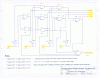
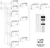
Hi, I want to Design, lay out, and simulate a CMOS four-input XOR gate in the standard
0.25 micron CMOS process. You can choose any logic circuit
style, and you are free to choose how many stages of logic to use: you
could use one large logic gate or a combination of smaller logic gates.
The supply voltage is set at 2.5 V! Your circuit must drive an external
20 fF load in addition to whatever internal parasitics are present in your
circuit.
The primary design objective is to minimize the propagation delay
of the worst-case transition for your circuit. The secondary objective is
to minimize the area of the layout. At the very worst, your design must
have a propagation delay of no more than 0.5 ns and occupy an area of
no more than 500 square microns, but the faster and smaller your circuit,
the better. Be aware that, when using dynamic logic, the precharge time
should be made part of the delay.
The design will be graded on the magnitude of A ´ tp
2, the product
of the area of your design and the square of the delay for the worst-case
transition.
help me
 
hello @turnglqvtv
Did you solve this problem?
"
Design, lay out, and simulate a CMOS four-input XOR gate in the standard
0.25 micron CMOS process. You can choose any logic circuit
style, and you are free to choose how many stages of logic to use: you
could use one large logic gate or a combination of smaller logic gates.
The supply voltage is set at 2.5 V! Your circuit must drive an external
20 fF load in addition to whatever internal parasitics are present in your
circuit.
The primary design objective is to minimize the propagation delay
of the worst-case transition for your circuit. The secondary objective is
to minimize the area of the layout. At the very worst, your design must
have a propagation delay of no more than 0.5 ns and occupy an area of
no more than 500 square microns, but the faster and smaller your circuit,
the better. Be aware that, when using dynamic logic, the precharge time
should be made part of the delay.
The design will be graded on the magnitude of A ´ tp
2, the product
of the area of your design and the square of the delay for the worst-case
transition.
"
 
An online search located two 14-pin DIP devices, one each from Texas Instruments and Fairchild/ On Semiconductor. Both have identical pinouts, neither device is a CMOS.
 
Status
Not open for further replies.

Latest threads

New Articles From Microcontroller Tips

Back
Top