I've a circuit using several NCP81151 fet drivers. The designer of this chip obviously loves pins doing more than one function, so the EN has three states. Low turns the driver circuit off, Mid makes signals go low and High lets the PWM decide. Here are the voltage values.

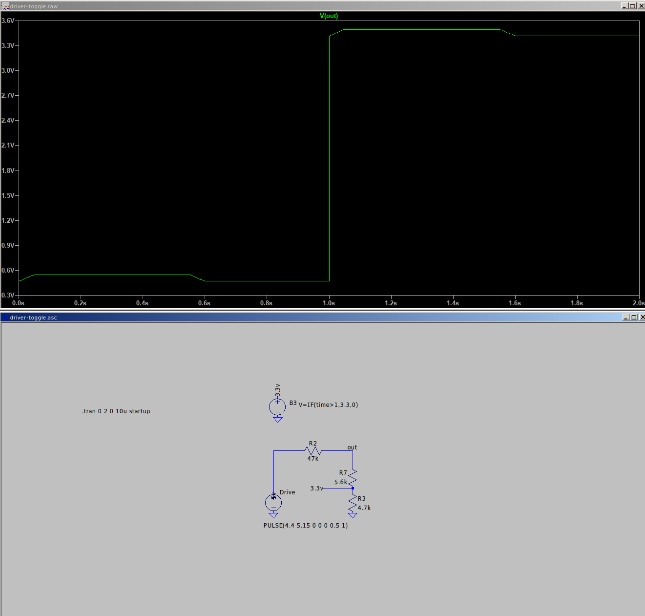
My control chip is an NRF52, so 3.3V max. I need to switch the circuit between Low and High (don't need Mid). It's easy enough to solve using a transistor or FET but floorspace is quite critical and I'd have to add 5 SOT-323's to do it. So I came up with a voltage divider and tested it in LTSpice. Using the voltage extremities for the 5V line it looks like I can just do it, with 0.1v to spare. Close but within spec.

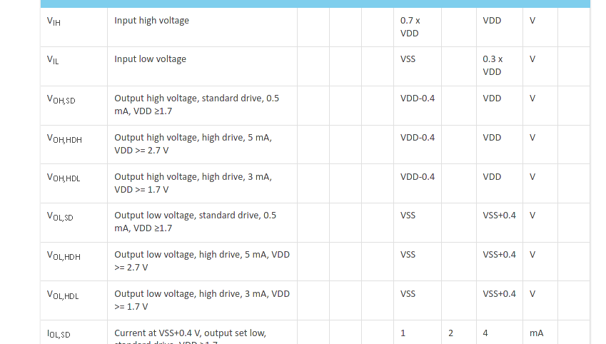
But here's the thing. I assumed (always the mother of all ****ups) the NRF52 was driving it's outputs using FETs, so as long as current draw was minimal there'd be no drop and I could assume a 0v and 3.3v swing. Going to the datasheet to verify this....

So my question is where does this +/- 0.4v come from? If it were a transistor driver I'd expect a 0.6-0.7v drop. The fact it can do VSS indicates it's FET based, but I have 0.1v of tolerance not 0.4v to play with so I need to know where this figure comes from to determine if my approach is going to work.
My control chip is an NRF52, so 3.3V max. I need to switch the circuit between Low and High (don't need Mid). It's easy enough to solve using a transistor or FET but floorspace is quite critical and I'd have to add 5 SOT-323's to do it. So I came up with a voltage divider and tested it in LTSpice. Using the voltage extremities for the 5V line it looks like I can just do it, with 0.1v to spare. Close but within spec.
But here's the thing. I assumed (always the mother of all ****ups) the NRF52 was driving it's outputs using FETs, so as long as current draw was minimal there'd be no drop and I could assume a 0v and 3.3v swing. Going to the datasheet to verify this....
So my question is where does this +/- 0.4v come from? If it were a transistor driver I'd expect a 0.6-0.7v drop. The fact it can do VSS indicates it's FET based, but I have 0.1v of tolerance not 0.4v to play with so I need to know where this figure comes from to determine if my approach is going to work.
