Continue to Site

Welcome to our site!

Electro Tech is an online community (with over 170,000 members) who enjoy talking about and building electronic circuits, projects and gadgets. To participate you need to register. Registration is free. Click here to register now.

  • Welcome to our site! Electro Tech is an online community (with over 170,000 members) who enjoy talking about and building electronic circuits, projects and gadgets. To participate you need to register. Registration is free. Click here to register now.

Schematic PCB review - Capacitive Touch Sensor AT42QT1012

BaJRan

New Member
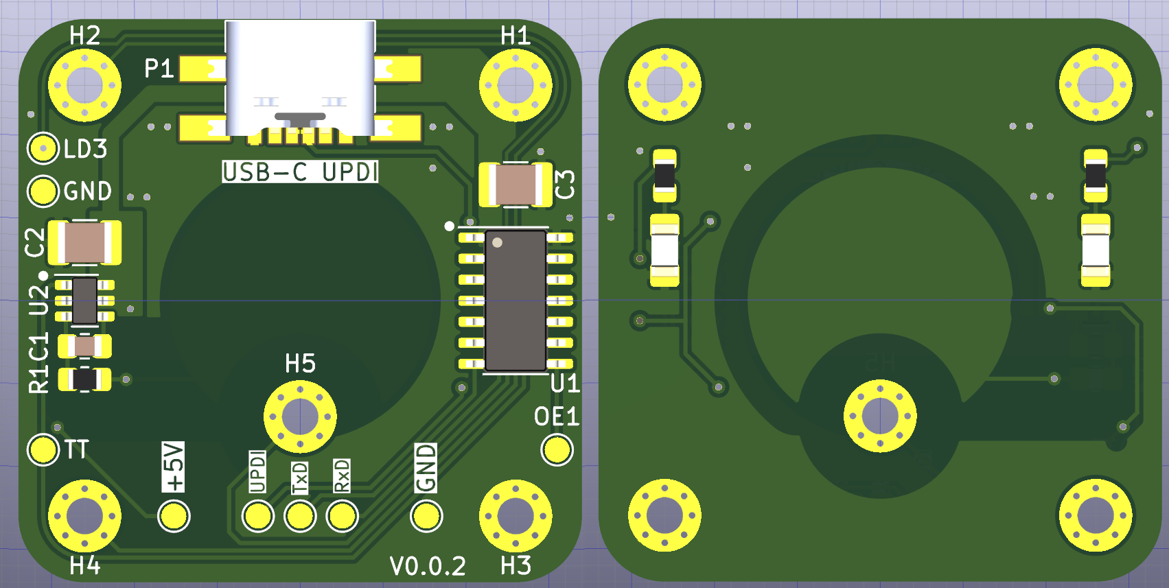
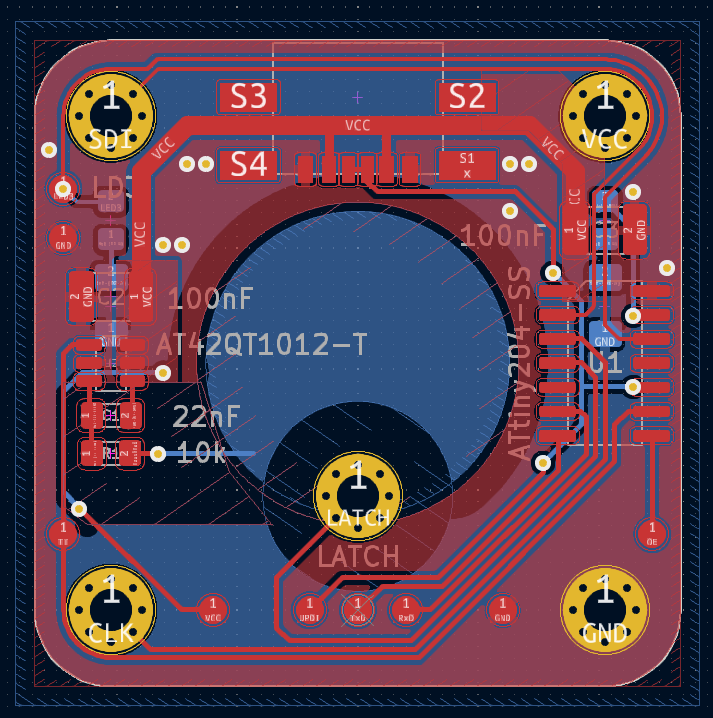
I designed a simple PCB for learning purposes. It consists of a touch sensor, Attiny microcontroller, and two LEDs. I have already soldered the PCB. I was able to program the Attiny microcontroller easily using MPLAB X IDE. I can control my two LEDs on the bottom side, but the touch sensor is not working correctly.

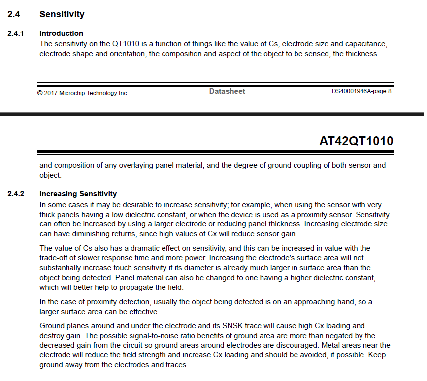
I would like to ask if I haven't made any major mistakes in the touch sensor area. I have attached the project in KiCad 8 and the datasheet for AT42QT1012

Best Regards,
Pawel
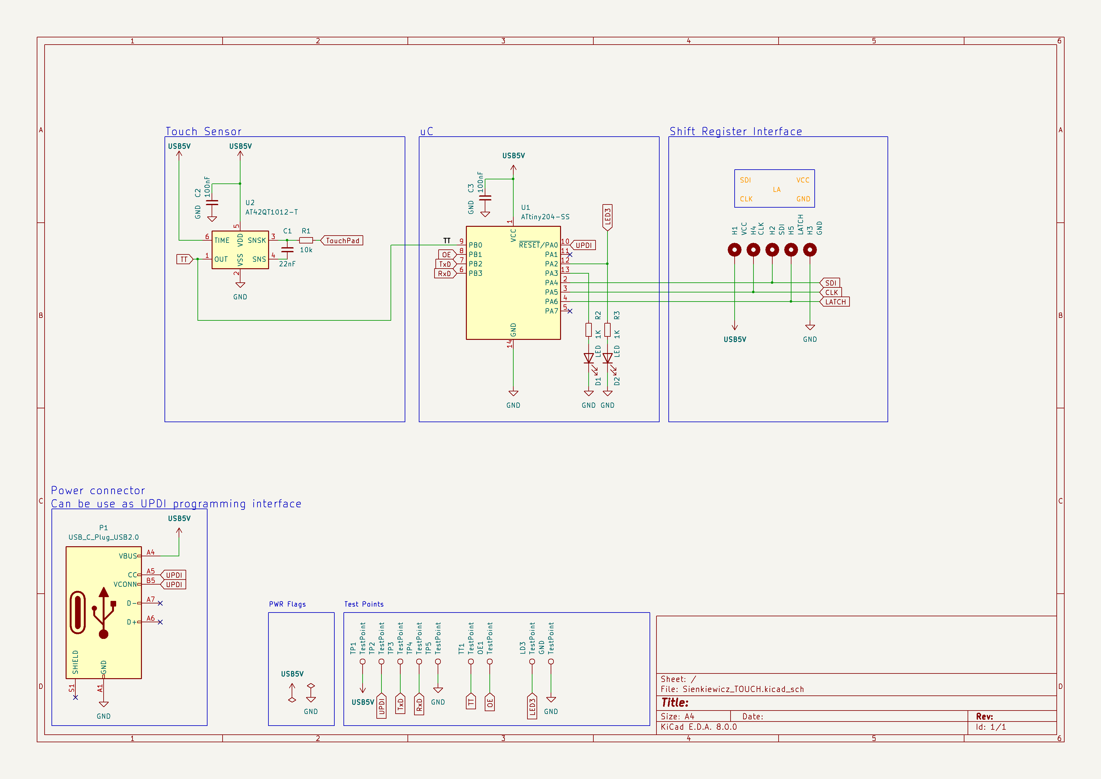
Schem1.png
PCB1.png
PCB2.png
Datascheet.png
 

Attachments

  • Sienkiewicz.zip
    144.9 KB · Views: 42
  • 40001946A.pdf
    264.4 KB · Views: 40
It is not a good layout for the touch pad. A good layout might be 2 interlocked combs with SNSK and GND interwoven or spiraled traces sp you can touch anywhere in the circle to bridge with 1mm of your finger tip for <1nF or a squashed fingertip of say 30 nF and a no touch capacitance of say, 100 pF.

I haven't done this or searched for examples but I would have used 0.1 mm tracks to SNSK with 2 interwoven spirals with a 1 mm gap and 0.2 mm track width max. and not a big circle pad. You don't want a large surface area antenna but rather low copper area with < 50% fill then to bridge the tracks anywhere in the circle with a 1xmm of skin or about 1nF. It could also be made so sensitive even a pointing a finger near the pad like a wand could work.

Increase Cs from 22 nF to 50 nF.

If that fails, then highlight all traces below in your gerber view to estimate all gaps and pF/mm and then we can compute your solution better.
1709768053170.png
 
Last edited:
You schematic might logically look like this.
But the twin electrodes could be meandering or co-spiral or interwoven combs, with a much wider gap (1mm )than the thinnest tracks 0.1 to 0.2 mm.

Then C1 can reduce the current limit applied thru 2 nF.
1709771963134.png
 
Looking at the App Note, they also use a large coin pad and not so close to ground. They say the touch capacitance would add 0.5 to 5pF. I read this to mean the pad dielectric to air from the finger touching the pad and not necessarily bridging the pad to ground. Thus the no load capacitance would be likely 0.1 pF for their 1sided layout with no other signals nearby!

I suggest you actually bridge the capacitance of signal to ground to conduct much higher than 100 pF to 1nF with a 1 to 2 mm of skin bridging the signal and ground. Of course dry skin will be much less and then will need more pressure.
1709773944213.png


If you can design a 1 ~2pF capacitor using coin sized PCB traces on 1 side, then you will understand what to do. Until then copy exactly what it says in App Note without any compromises to the exact sizes you see away from any other signals. Otherwise ask measurement questions.
 
Last edited:

Latest threads

New Articles From Microcontroller Tips

Back
Top