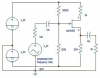
Continue to Site

Welcome to our site!

Electro Tech is an online community (with over 170,000 members) who enjoy talking about and building electronic circuits, projects and gadgets. To participate you need to register. Registration is free. Click here to register now.

  • Welcome to our site! Electro Tech is an online community (with over 170,000 members) who enjoy talking about and building electronic circuits, projects and gadgets. To participate you need to register. Registration is free. Click here to register now.

p-channel JFET calculation

Status
Not open for further replies.

aabundle

New Member
Hey guys,

Ive been tring (over the past week) to try and get a p-channel amp just work to bias on properly. I can get a n-type to work properly but every time i try the p-type i get no gain on my output.

The text book and my class notes say "the same equations apply" blah blah but i cant get any results in simulation and its giving me headaches.

The equations i have are:

Id = K((Vgs-Vtr)^2)

then you solve for Id and choose the suitable current.

Then check the fet isn't in triode region.

I just cant get any combination to work with the p-type.

Can you guys offer any help. Should the output be on the drain or the source for the p-type?

Cheers

hi,
There are 'enhancement' and 'depletion' type jFET's, what are the type numbers you are using.?
 
Hey,

Im using a 2N5460 general purpose amp

its pinch off voltage range is (Vgsoff) = 0.75 - 5 v

Idss range is = -1 to -5 mA

im using sabre to simulate the circuits.
 
For example.

**broken link removed**

with this CCT i do the following calculations

p type j-FET Characteristics (Vp = 2.5, Idss = 30mA (Sabers value))

I choose a Id = 2.5 mA (which seems pretty reasonable)

then working backwards from the saturation formula:

Id = (Idss/Vp)(Vgs - Vp)^2

i get a value for Vgs = 2v which is under Vp = 2.5v

So then i make the bias over the 12/-12 supply be +5v for Vg

And then i want Vgs of 2v so i make the source resistor 3.6k so 3v is at Vs.

Then i make Rd 3k so saturation mode can be miantained.

But then i run the simulation and the output is less than the input.

have i made a mistake with my calculations?
 
hi aa,
Been looking at your circuit, I will try your tests using LTspice, later today, get back to you you.
 
Looks like you using a positive power supply. It should be negative for a P-Channel.
 
Looks like you using a positive power supply. It should be negative for a P-Channel.

Hi Carl,
This what I also noticed.
The datasheet is a little ambiguous.???
 

Attachments

  • MM_MMBF5460.pdf
    114.9 KB · Views: 247
It's a P-Channel depletion-mode device (which most J-FETs are) so it normally operates with a negative drain-source voltage and a positive gate-source voltage. The required positive gate source bias voltage can be generated with a source resistor to ground and the gate grounded through a resistor. You select the source resistor to give the desired (gate to) source voltage at the design drain operating current.
 
neither have I, but we keep getting new stuff all the time, and I don't mean better microprocessors. I've met 2 new components this week and I don't expect that to stop just because I'm getting old.
 
I wouldn't worry about enhancement JFETs, they'll probably be invented after the depletion mode BJT. :rolleyes:
 
Looks like you using a positive power supply. It should be negative for a P-Channel.

Hey im using a 12/-12 power supply. I have set the bais on the base so the Vgs is less than the pich off voltage,

So do i have to have an actual -ve voltage on the gate or a Vgs that is lower than the pinch off voltage
 
The split supply has no effect on the polarity to the FET. The FET just seems the combined voltage of the two supplies in series.

Which is the drain and which is the source in your schematic? The designators are blurry.
 
Last edited:
You made a negative schematic picture so I inverted it for normal black lines on a white background.
You made it so big that it didn't fit in my neighbourhood so I cropped it.
You saved it as a fuzzy JPG file type so I couldn't make it clear.

Your Jfet has such a high value unbypassed source resistor that it has a high voltage loss instead of some gain.
 

Attachments

  • Jfet circuit cropped.PNG
    Jfet circuit cropped.PNG
    47.8 KB · Views: 295
Last edited:
I wouldn't worry about enhancement JFETs, they'll probably be invented after the depletion mode BJT. :rolleyes:

hero,
Look at 2N3819 njFET and the 2N3820 pjFET. [ they are in the LTS library]

The 2N3819 is often used in scope and VHF front end amps because of its wide freq spec.

They also make excellent constant current sources with virtually no tempr effect problems.
 

Attachments

  • 70596.pdf
    52.1 KB · Views: 142
Looks like you using a positive power supply. It should be negative for a P-Channel.

Hey Carl,

The power supply doesn't have to be negative for the p-type. Vgs has to be negative and below the pinch off voltage, according to the text book. So allowing Vs to be bigger than Vg should satisfy this condition.

as Vgs = Vg - Vs
 
Last edited:
You made a negative schematic picture so I inverted it for normal black lines on a white background.
You made it so big that it didn't fit in my neighbourhood so I cropped it.
You saved it as a fuzzy JPG file type so I couldn't make it clear.

Your Jfet has such a high value unbypassed source resistor that it has a high voltage loss instead of some gain.

Thanks, im just re-working my calculations,i will re-post a better diagram.
 
Status
Not open for further replies.

Latest threads

New Articles From Microcontroller Tips

Back
Top