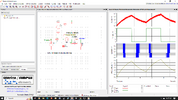
Folks seem to like building delays, debounce keys, etc, by placing large C at the
inputs to CMOS gates.
NOT A GOOD IDEA
For case where supply collapse rapid due to its design, load situation.
TI confirms this in an ap note on general CMOS usage. Here is a rough sim of the problem.
Note since spice model did not have the parasitic diodes in it I used external as substitute.
Also used 1 ohm as C ESR......roll your own value(s) for your case. Note using .1 ohms for
C ESR produced 3A thru D1......

The simple way around this is to place a series R between gate input and the large C.
Regards, Dana.
inputs to CMOS gates.
NOT A GOOD IDEA
For case where supply collapse rapid due to its design, load situation.
TI confirms this in an ap note on general CMOS usage. Here is a rough sim of the problem.
Note since spice model did not have the parasitic diodes in it I used external as substitute.
Also used 1 ohm as C ESR......roll your own value(s) for your case. Note using .1 ohms for
C ESR produced 3A thru D1......
The simple way around this is to place a series R between gate input and the large C.
Regards, Dana.
Last edited: