Continue to Site

Welcome to our site!

Electro Tech is an online community (with over 170,000 members) who enjoy talking about and building electronic circuits, projects and gadgets. To participate you need to register. Registration is free. Click here to register now.

  • Welcome to our site! Electro Tech is an online community (with over 170,000 members) who enjoy talking about and building electronic circuits, projects and gadgets. To participate you need to register. Registration is free. Click here to register now.

how to initialize LCD 16x2

Status
Not open for further replies.
I've normally found just connecting the V0 to Gnd is good enough. Disconnect the LED and it should look fine.

Mike.

When I turn off the LED, only the black box is visible and as far as I know character should be displayed on LCD.
 
Read the datasheet.. You may need a negative voltage If your Vo needs to be negative, you'll need a 7660 charge pump to generate -5v..

Have there been any LCD modules that needed a -ve supply this century? - or even in the later years of the previous one?.

I know historically the very early ones needed a negative supply, but I don't think I've ever seen one?.

Thinking on, I doubt there was ever one with LED backlighting that required a negative voltage?.
 
I have these two LCD module
 

Attachments

  • IMG_20201006_170614.jpg
    IMG_20201006_170614.jpg
    190.5 KB · Views: 180
  • IMG_20201006_170718.jpg
    IMG_20201006_170718.jpg
    514.4 KB · Views: 185
You don't seem able or unwilling to answer simple questions. My troll radar has peaked. Bye.

Mike.
 
You don't seem able or unwilling to answer simple questions. My troll radar has peaked. Bye.

Mike.
I'm newbie I don't have much experience in electronics field Your question is not clear for me. Generally VO means output voltage for me. I did not understand on which pin you want to check voltage
 
Yes, V0 mentioned on page 1 but you're confused on page 3. Don't want you to check any pin. Have a good life.

Mike.
 
A few comments, some of which will echo what others have said...

In one of the pictures, sensible text can be seen faintly on the LCD, so the program is working.

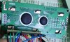
The backlight is far too bright, I suspect that the LEDs in the display module are connected directly to the +5v supply.
Look at the picture of the board, there is a connector for the LCD which is not being used, there are pins marked BL+ and BL-, these are for the backlight.
Whether there is a current limiting resistor somewhere on the development board I do not know, the board manufacturer does not appear to publish the user manual other than as a printed version supplied with the dev board.
As a temporary measure just disconnect the backlight, depending on the type of LCD, it will still be visible.

There is a potentiometer marked as CONTRAST ADJUST, I guess that this is connected to the CONT pin on the LCD connector.
Looking at the pictures, this appears to be connected to some power supply point. A very bad idea.

Lcd 1 pin connected gnd onboard
Lcd 2 pin connected to 5v onboard
Lcd 3 pin connected to gnd onboard
Wrong!

Just wire the contrast potentiometer correctly.

JimB
 
So, problem fixed, no more thread needed.

Mike.
Just one problem fixed. Now I know that my hardware is working correctly. Now I want to test code which I have written myself.
I am not getting data on LCD when I run my code in post #9. Now I am trying to find out what is wrong in my code due to which I am not getting data on LCD

IMG_20201006_180657.jpg
 
Now first I have to fix the LCD initlization function for 4 bit mode. I'm just trying to fix this function

Hi Ritesh, the sole ability you exhibit is quickly firing questions after questions.

Sure I am not going to make the mistake to follow any of your threads in the future.
 
Hi Ritesh, the sole ability you exhibit is quickly firing questions after questions.

Sure I am not going to make the mistake to follow any of your threads in the future.
Already You are on my ignor list in ACC because of your behaviour. You don't respect forum members. You are the one who is trying to spoil someone's image. This is the second time you are talking nonsense. I have warned you even before this.

I will request the moderator I never want to see his post again
 
Last edited:
Hi Ritesh, the sole ability you exhibit is quickly firing questions after questions.
Sure I am not going to make the mistake to follow any of your threads in the future.

Already You are on my ignor list in ACC because of your behaviour. You don't respect forum members. You are the one who is trying to spoil someone's image. This is the second time you are talking nonsense. I have warned you even before this.

Hey, cool it guys!

ATF, this guy is not a reincarnation of Ritesh (as far as I can tell), so lay off him please.

Djsarkar, you do not seem to be able or willing to give feedback when asked by those trying to help you.
Please don't be surprised when some people become annoyed.

Lets cool it and play nicely.

JimB
 
I have a spent a lot of time to understand datasheet and as per my knowledge I have written code but still my program is not working

I don't see the text on the screen so can anyone point out what's wrong with code?

PORT D4 - LCD Data pin 4
PORT D5 - LCD Data pin 5
PORT D6 - LCD Data pin 6
PORT D7 - LCD Data pin 7

PORT RC4 - RS
PORT RC5 - RW
PORT RC6 - EN

C:
#define _XTAL_FREQ 8000000
#include <xc.h>
// PIC18F45K80 Configuration Bit Settings
// 'C' source line config statements
// CONFIG1L
#pragma config RETEN = OFF      // VREG Sleep Enable bit (Ultra low-power regulator is Disabled (Controlled by REGSLP bit))
#pragma config INTOSCSEL = HIGH // LF-INTOSC Low-power Enable bit (LF-INTOSC in High-power mode during Sleep)
#pragma config SOSCSEL = HIGH   // SOSC Power Selection and mode Configuration bits (High Power SOSC circuit selected)
#pragma config XINST = OFF       // Extended Instruction Set (Enabled)
// CONFIG1H
#pragma config FOSC = INTIO2    // Oscillator (Internal RC oscillator)
#pragma config PLLCFG = OFF     // PLL x4 Enable bit (Disabled)
#pragma config FCMEN = OFF      // Fail-Safe Clock Monitor (Disabled)
#pragma config IESO = OFF       // Internal External Oscillator Switch Over Mode (Disabled)
// CONFIG2L
#pragma config PWRTEN = OFF     // Power Up Timer (Disabled)
#pragma config BOREN = SBORDIS  // Brown Out Detect (Enabled in hardware, SBOREN disabled)
#pragma config BORV = 3         // Brown-out Reset Voltage bits (1.8V)
#pragma config BORPWR = ZPBORMV // BORMV Power level (ZPBORMV instead of BORMV is selected)
// CONFIG2H
#pragma config WDTEN = OFF      // Watchdog Timer (WDT disabled in hardware; SWDTEN bit disabled)
#pragma config WDTPS = 1048576  // Watchdog Postscaler (1:1048576)
// CONFIG3H
#pragma config CANMX = PORTB    // ECAN Mux bit (ECAN TX and RX pins are located on RB2 and RB3, respectively)
#pragma config MSSPMSK = MSK7   // MSSP address masking (7 Bit address masking mode)
#pragma config MCLRE = ON       // Master Clear Enable (MCLR Enabled, RE3 Disabled)
// CONFIG4L
#pragma config STVREN = ON      // Stack Overflow Reset (Enabled)
#pragma config BBSIZ = BB2K     // Boot Block Size (2K word Boot Block size)
// CONFIG5L
#pragma config CP0 = OFF        // Code Protect 00800-01FFF (Disabled)
#pragma config CP1 = OFF        // Code Protect 02000-03FFF (Disabled)
#pragma config CP2 = OFF        // Code Protect 04000-05FFF (Disabled)
#pragma config CP3 = OFF        // Code Protect 06000-07FFF (Disabled)
// CONFIG5H
#pragma config CPB = OFF        // Code Protect Boot (Disabled)
#pragma config CPD = OFF        // Data EE Read Protect (Disabled)
// CONFIG6L
#pragma config WRT0 = OFF       // Table Write Protect 00800-01FFF (Disabled)
#pragma config WRT1 = OFF       // Table Write Protect 02000-03FFF (Disabled)
#pragma config WRT2 = OFF       // Table Write Protect 04000-05FFF (Disabled)
#pragma config WRT3 = OFF       // Table Write Protect 06000-07FFF (Disabled)
// CONFIG6H
#pragma config WRTC = OFF       // Config. Write Protect (Disabled)
#pragma config WRTB = OFF       // Table Write Protect Boot (Disabled)
#pragma config WRTD = OFF       // Data EE Write Protect (Disabled)
// CONFIG7L
#pragma config EBTR0 = OFF      // Table Read Protect 00800-01FFF (Disabled)
#pragma config EBTR1 = OFF      // Table Read Protect 02000-03FFF (Disabled)
#pragma config EBTR2 = OFF      // Table Read Protect 04000-05FFF (Disabled)
#pragma config EBTR3 = OFF      // Table Read Protect 06000-07FFF (Disabled)
// CONFIG7H
#pragma config EBTRB = OFF      // Table Read Protect Boot (Disabled)

#define RS            LATCbits.LATC4
#define RW            LATCbits.LATC5
#define EN            LATCbits.LATC6

#define LCD_Port      LATD

void Port_pins_Initialized (void)
{
    LATA = LATB = LATC = LATD = LATE =  0;
    TRISA = 0b0000000;// all are output, Unused
    TRISB = 0b0000000;// all are output, Unused
    TRISC = 0b0000000;// RS RW EN
    TRISD = 0b0000000;//  LCD
    TRISE = 0b0000000;// All are output, Unused

    ANCON0 = 0; // digital port
    ANCON1 = 0; // digital port
    CM1CON = 0; // Comparator off
    CM2CON = 0; // Comparator off
    ADCON0 = 0; // A/D conversion Disabled
}

void LCD_E_Pulse(void)
{
    EN = 1;
    __delay_us(4);
    EN = 0;
    __delay_us(4);
}

void LCD_WriteCmd(unsigned char data)
{
    RS = 0; RW = 0;
    LCD_Port = data & 0xF0 ;  // send upper nibble
    LCD_E_Pulse();

}

void LCD_WriteData(unsigned char data)
{
    RS = 1; RW = 0;
    LCD_Port = data & 0xF0 ;  // send upper nibble
    LCD_E_Pulse();
    __delay_ms(20);
    LCD_Port = (data << 4 ) & 0xF0 ;  // send lower nibble
    LCD_E_Pulse();

}


void buffer( unsigned char *p)
{

    while (*p != '\0')
    {
      LCD_WriteData(*p);

        p++;
    }
}

void LCD_Init(void)
{
    __delay_ms(15);
    LCD_WriteCmd(0x30);
    __delay_ms(5);
    LCD_WriteCmd(0x30);
    __delay_us(40);
    LCD_WriteCmd(0x30);
    __delay_us(40);
    LCD_WriteCmd(0x20);
    __delay_us(40);
    LCD_WriteCmd(0x20);
    __delay_us(40);
    LCD_WriteCmd(0x20);
    __delay_us(40);
    LCD_WriteCmd(0x00);
    __delay_us(40);
     LCD_WriteCmd(0x80);
    __delay_us(40);
    LCD_WriteCmd(0x00);
    __delay_us(40);
    LCD_WriteCmd(0x10);
    __delay_us(40);
    LCD_WriteCmd(0x00);
    __delay_us(40);
    LCD_WriteCmd(0x70);
    __delay_us(40);
  
}

void main ()
{
  
   unsigned int i = 0;
   unsigned char Data1 [20]="Hello World";
   Port_pins_Initialized();
   LCD_Init();
   buffer(Data1);

  
     while (1)
     {

    
     }
}
 
Last edited:
The writecommand is only writing the high nibble. After the first few commands you need to write both nibbles. Do as it says in the datasheet. Note in the table, after writing 2 it then writes in pairs.


Mike.
 
Status
Not open for further replies.

Latest threads

New Articles From Microcontroller Tips

Back
Top