Electro Tech is an online community (with over 170,000 members) who enjoy talking about and building electronic circuits, projects and gadgets. To participate you need to register. Registration is free. Click here to register now.
Welcome to our site! Electro Tech is an online community (with over 170,000 members) who enjoy talking about and building electronic circuits, projects and gadgets. To participate you need to register. Registration is free. Click here to register now.
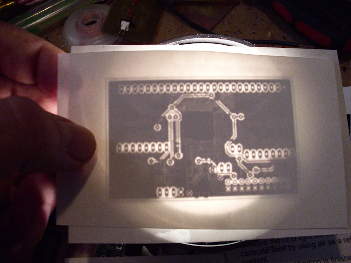
I wanted to try double sided PCB using toner transfer method. I printed out the top and bottom copper. My question is how to align the printed top and bottom on the PCB sides so that via holes and others are aligned? any tricks and tips?
I wanted to try double sided PCB using toner transfer method. I printed out the top and bottom copper. My question is how to align the printed top and bottom on the PCB sides so that via holes and others are aligned? any tricks and tips?
Hi,
I've been making film copies of each side SVG (Keeps image the correct size) then make up a (in my case) 4"x6" x PCB thickness" appr 10mm wide, 'L' square out of card. Place the two films together lining up the circuit, then glue the square between the films, along bottom and side. place PCb up to the square, and pinch all together when turning over on the light box.
I'm just going to look at the Laser print/heat method. (making the films is a bit time consuming)
Camerart.
I drill a few vias through a printout and the blank board, I use a pin to punch the same holes in the top and bottom toner prints, I use thin wire or fishing line to align them to the blank drilled brd, then tape before I heat-press them.
If you look at the video you will see square corners which are basically a no no for circuit boards.
I have a well explained tutorial on Electro tech online as well as over at Digital DIY. Have made lots of double sided boards.
Will try and locate the tutorial
Just skipped through the video, but I think he is doing it like I used to do it. Just print out the two images, line them up using a bright light shining through and then tape the paper together so it doesn't move. Slip the PCB between and iron, everything should be lined up. Took a series of images a few years ago that someone was going to make into a tutorial, but it never happened.
I found using stick pins on the corners works well then tape together before laminating
or better yet laminate one side, stick the pins in the holes you drilled for alignment.
line up side 2 and use the pins for alignment. this method works even better.
I wanted to try double sided PCB using toner transfer method. I printed out the top and bottom copper. My question is how to align the printed top and bottom on the PCB sides so that via holes and others are aligned? any tricks and tips?
EDIT: I quote from the build instructions section on dbl sided registration: For double sided boards with thru hole parts: Place a TTF print face up on the board and align to take strips of painter's tape along the 5mm border. Secure with bits of tape on the sides. Now use a large safety pin or the pin cap from a Krazy Glue tube, carefully press a pinpoint punch mark in the centre of any thru hole pads near the corners of the layout so the copper clad is marked. I usually add custom pad/vias just for this purpose, perimeter machine screw locations are good as well. Once you have 3 or 4 corners marked, carefully remove the TTF print and use a regular 'bobby' pin to pass thru each punched hole in the TTF. Now take the other TTF layer print and carefully punch thru the SAME pads with the bobby pin. I use a bit of backing cardboard to do this easily. It is important to punch the centres of all the pads you choose. Using a 0.8mm drill, carefully drill the registration punch marks you made on the copper clad.
If you're designing double sided boards you'll want to have a few holes somewhere that you can use to align both sides. I usually add an extra centimeter around the edge and put a small hole in each corner. The most important thing is to fill in all blank areas black it will make easier to iron and harder to rip/crease while sticking to the board.
I've only done the UV exposure method double sided. I used 4 thumbtacks, one in each corner, to align the masks.
At the time (work), I had the ability to spin coat the resist and bake in a "yellow room". The holes slightly messed up the uniformity of the resist since they were drilled prior to coating. Moving the drill press from the machine shop wasn't an easy option.
I keep mentioning that I used the surface tension of water (a drop) to keep the photographic mask against the board instead of a glass plate.
I just tape my transparencies together on the ends after aligning them. Then slip the board between the sleeve. I use window glass to press everything together. I prefer to have the pigment side of the transparency next to the PCB and I have recently switched back to an ink jet printer for those. Water might cause smearing.
This site uses cookies to help personalise content, tailor your experience and to keep you logged in if you register.
By continuing to use this site, you are consenting to our use of cookies.

") .
.