Electronic Projects, forums and more.

Go Back   Electronic Circuits Projects Diagrams Free > Electronics Forums > General Electronics Chat


General Electronics Chat This forum is for general chat about electronics, eg: Dont know what a part does? Dont know how to read a circuit? Want to get an opinion?

Reply
 
LinkBack Thread Tools Display Modes
Old 16th December 2006, 07:10 PM   (permalink)
Default Double sided PCBs in Eagle

Hi there,

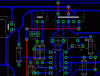
Doing double sided PCBs in CAD software like Eagle or Electronicsworkbench makes som problems for the hobbyist with no access to through hole plating machinery. When autorouting a double sided PCB the software make holes for components into vias. It means that you either have to make through hole plating to get the proper connection between the layers or solder the components on both sides. The first technique is quite expensive (and time-consuming) and the other a very bad idea.

Is it possible to set-up the software so that it doesn't use holes as vias, so the connections between the layers can be done with a piece of wire?

If that's not possible, could anyone then tell me how to make my own via on a PCB trace and make my own PCB traces manually, so I can manually solve the problem after autorouting?
Electronics4you is offline  
Old 16th December 2006, 07:33 PM   (permalink)
Default

Quote:
Originally Posted by Electronics4you
It means that you either have to make through hole plating to get the proper connection between the layers or solder the components on both sides. The first technique is quite expensive (and time-consuming) and the other a very bad idea.
why is it 'very bad' to solder components on both sides?

Quote:
If that's not possible, could anyone then tell me how to make my own via on a PCB trace and make my own PCB traces manually, so I can manually solve the problem after autorouting?
I've never used the autorouter, even on complex double sided boards ... there's a certain sense of accomplishment to doing it yourself, not to mention the micromanager in me loves the fiddley work.

use the ROUTE command to draw your own traces, it looks like two green dots connected with a red line
__________________
If you don't have a planet, what good are gold bars?

want to contact me directly? gmail gordonthree
check out my project website: http://projects.dimension-x.net
Favorite numbers:
09 F9 11 02 9D 74 E3 5B D8 41 56 C5 63 56 88 C0
justDIY is offline  
Old 16th December 2006, 07:50 PM   (permalink)
Default

If you close the schematic and leave the board open, you can do anything you like to the board (Eagle stops trying to go back to the schematic).

Sometime you have to use the group tool to move things though. You just can not annotate back to the schematic at that point (so your schematic better be done at that point). I friend of mine goes in, makes an empty schematic, click PCB, closes the schematic and does the whole thing in PCB mode.

Me, I do schematic and then PCB and then leave pleny of space, LET Eagle route it, and shrink it all up. I am not a PCB guy and normally in a hurry. And I have learned enough to do it by hand, but time is short for me
mramos1 is offline  
Old 16th December 2006, 08:19 PM   (permalink)
Default

Soldering components on both sides is hard to do without buring som components especially on close component boards. The un-soldering proces is even harder to accomplish.

I'm always in a hurry, and don't have the time (even if I want to do PCB routing all day) to do it, because the development and analysis of the circuit afterwards is a heavy job.

Can you just make a via where you want and then move the "left-over trace" to the next layer?
Electronics4you is offline  
Old 16th December 2006, 08:33 PM   (permalink)
Default

Quote:
Originally Posted by Electronics4you
Soldering components on both sides is hard to do without buring som components especially on close component boards. The un-soldering proces is even harder to accomplish.

I'm always in a hurry, and don't have the time (even if I want to do PCB routing all day) to do it, because the development and analysis of the circuit afterwards is a heavy job.

Can you just make a via where you want and then move the "left-over trace" to the next layer?
If you close the schematic windows you can alter the PCB in any way you like. I do boards all the time where I close the schematic and drop larger pads over the old small ones all the time, because I (am lazy) did not search the forum here to see how to set and save the defaults
mramos1 is offline  
Old 17th December 2006, 12:32 AM   (permalink)
Default

You can tell eagle how many vias it's allowed to use to minimize it going nuts with the autorouter (Tools/Auto). Then you can "tear up" any traces you don't like and route them yourself.
You can also just tell eagle to do a single sided board only (Tools/Auto) by setting N/A as the top layer. Then you can just add pads for the unrouted traces for topside jumper wires.
__________________
--- The days of the digital watch are numbered. ---
kchriste is offline  
Old 17th December 2006, 04:06 AM   (permalink)
Default

when you're using the ROUTE command, you can change layers on the fly, and eagle will automatically generate a via at that location. When I'm in a rush, I use this method, instead of specifying jumpers in the schematic.
__________________
If you don't have a planet, what good are gold bars?

want to contact me directly? gmail gordonthree
check out my project website: http://projects.dimension-x.net
Favorite numbers:
09 F9 11 02 9D 74 E3 5B D8 41 56 C5 63 56 88 C0
justDIY is offline  
Reply

Bookmarks

Thread Tools
Display Modes


Similar Threads
Title Starter Forum Replies Latest
Double sided copper boards Screech General Electronics Chat 10 26th February 2007 09:02 AM
:: Double Sided PCB - Never Made 1 Before :: suby786 General Electronics Chat 4 26th November 2006 10:12 PM
Eagle - How to make Single Sided PCB elexhobby Electronic Projects Design/Ideas/Reviews 5 14th October 2005 05:24 PM
Difference between double sided PCB and 2 layer PCB darvaish Electronic Projects Design/Ideas/Reviews 2 10th March 2005 06:32 PM
how to solder properly tight areas for double side pcb's? spyghost Electronic Projects Design/Ideas/Reviews 8 23rd April 2004 02:02 AM


All times are GMT. The time now is 04:57 PM.


Electronic Circuits  |  Learning Electronics
Powered by vBulletin® Version 3.7.0
Copyright ©2000 - 2008, Jelsoft Enterprises Ltd.

eXTReMe Tracker