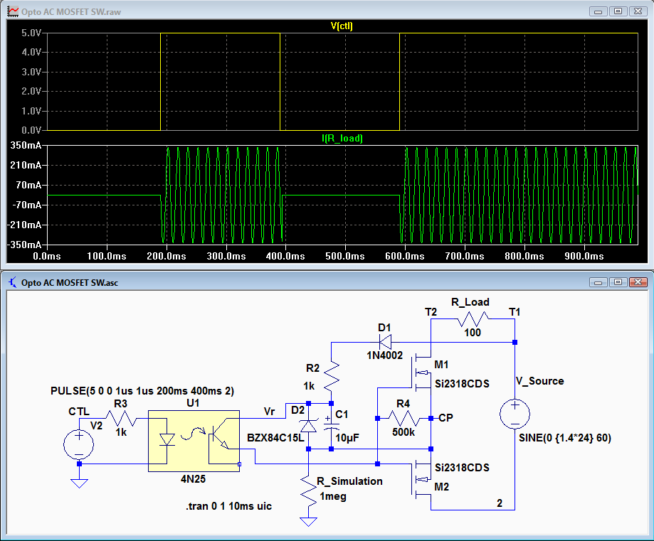
Here is a basic isolated-input, solid-state relay that uses two back-to-back MOSFETs for on/off load control from either an AC or DC supply.
As shown below, two N-MOSFETs are connected source-to source so that they can block voltage in either direction when OFF.
When their gates are biased ON they will switch a load from either an AC or DC supply (V_Source) since MOSFETs conduct equally well in either direction when ON.
(Note that V_Source polarity must be as shown for DC to provide proper biasing of the MOSFETs)

MOSFETs have an efficiency advantage over SCRs for switching AC current since their conducting voltage drop, and thus power dissipation, can be made much lower than an SCR's (whose drop is typically over a volt), as determined by a power MOSFET's generally low ON resistance.
But MOSFETs don't have the zero-voltage turn-off characteristic that SCRs do, if that's important to your application.
The maximum voltage drop, current, and switched voltage is determined by the selected MOSFET type.
If MOSFETs are selected with an ON resistance low enough to keep the MOSFET dissipation below about a watt or so (depending upon the MOSFET's package style) at the maximum load current, then the MOSFETs won't need a heatsink.
The MOSFET must be selected for the minimum supply voltage. If the peak supply voltage is below 11V then a logic-level type MOSFET must be used whose ON resistance is specified at the peak supply voltage minus 1 volt.
The circuit consists of an opto-isolator controlling the gate voltage to two N-MOSFETs connected source-to-source, with their sources used as the common point (CP) for the control circuit. The output is galvanically isolated from the input control signal.
(R_Simulation is there only to get the simulation to run and is not needed in a real circuit).
D1 is a half-wave rectifier that generates the DC voltage to control the MOSFET's gates.
The return path for the current is provided by the M2 MOSFET substrate diode.
The 15V zener diode D2 regulates the voltage to 15V and C1 smooths the voltage.
The LTspice simulation of the circuit below for a 24Vrms AC source, shows the on/off current flow through the load resistor as controlled by the CTL input signal to the opto-isolator.
The maximum switching frequency of the CTL input is determined by the opto-isolator's switching characteristics, and the value of R4 (which has to discharge the large MOSFET gate charge).
As shown below, two N-MOSFETs are connected source-to source so that they can block voltage in either direction when OFF.
When their gates are biased ON they will switch a load from either an AC or DC supply (V_Source) since MOSFETs conduct equally well in either direction when ON.
(Note that V_Source polarity must be as shown for DC to provide proper biasing of the MOSFETs)
MOSFETs have an efficiency advantage over SCRs for switching AC current since their conducting voltage drop, and thus power dissipation, can be made much lower than an SCR's (whose drop is typically over a volt), as determined by a power MOSFET's generally low ON resistance.
But MOSFETs don't have the zero-voltage turn-off characteristic that SCRs do, if that's important to your application.
The maximum voltage drop, current, and switched voltage is determined by the selected MOSFET type.
If MOSFETs are selected with an ON resistance low enough to keep the MOSFET dissipation below about a watt or so (depending upon the MOSFET's package style) at the maximum load current, then the MOSFETs won't need a heatsink.
The MOSFET must be selected for the minimum supply voltage. If the peak supply voltage is below 11V then a logic-level type MOSFET must be used whose ON resistance is specified at the peak supply voltage minus 1 volt.
The circuit consists of an opto-isolator controlling the gate voltage to two N-MOSFETs connected source-to-source, with their sources used as the common point (CP) for the control circuit. The output is galvanically isolated from the input control signal.
(R_Simulation is there only to get the simulation to run and is not needed in a real circuit).
D1 is a half-wave rectifier that generates the DC voltage to control the MOSFET's gates.
The return path for the current is provided by the M2 MOSFET substrate diode.
The 15V zener diode D2 regulates the voltage to 15V and C1 smooths the voltage.
The LTspice simulation of the circuit below for a 24Vrms AC source, shows the on/off current flow through the load resistor as controlled by the CTL input signal to the opto-isolator.
The maximum switching frequency of the CTL input is determined by the opto-isolator's switching characteristics, and the value of R4 (which has to discharge the large MOSFET gate charge).


