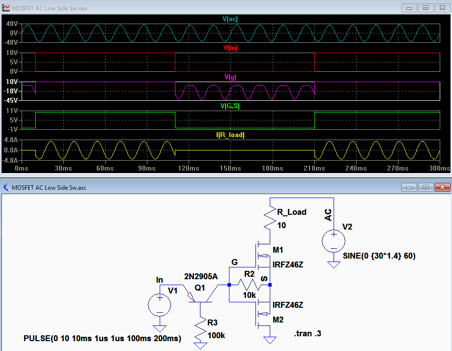
Here's a circuit that uses two back-to-back N-MOSFETs and one PNP BJT to form a low-side bipolar switch for either AC or plus/minus DC sources.
This has much lower On voltage drop and power loss than a TRIAC (for example a Triac will typically dissipate >10W at 10Arms current whereas the two MOSFETs will dissipate a total of <1W for low ON resistance MOSFETs at the same current).
The circuit also doesn't latch on with a DC source as a TRIAC does.
It can be used in place of an SSR when the AC/DC voltage source is already isolated from the Mains by a transformer and thus isolation for the control signal is not required.
The circuit takes advantage of the fact that a MOSFET conducts equally well in both directions when biased ON.
Two back-to-back N-MOSFETs are used to allow blocking for both polarities of the supply source (otherwise the parasitic MOSFET substrate diode would conduct in the reverse direction.)
The common-base configured PNP allows the positive control voltage to turn on the MOSFETs, but blocks the negative voltages (Vg, purple trace below) that occur at the gate from the gate-source connection when the control signal is 0V (giving Vg,s = 0V) and the supply voltage goes negative.
The input ON control voltage must be equal to the Vgs voltage for which the ON resistance, Rds(on), is specified in the MOSFET spec sheet.
This is typically 10V for standard MOSFETs and 5V (or less) for logic-level type MOSFETs.
The maximum allowed peak AC or DC voltage is determined by the voltage ratings of the MOSFETs and the PNP transistor (whichever is lower).
For inductive loads, back-to-back zeners or other transient suppressors will need to be used from the drain of M1 to ground, to limit the peak voltage to at least 25% below the ratings of the transistors.
The LTspice simulation below shows the current through the load resistor R_Load, for high (ON) and zero (OFF) input voltages and a 30Vrms AC source voltage.
The ON voltage drop equals the load current times twice the ON resistance of the MOSFET type selected.
