Continue to Site

Welcome to our site!

Electro Tech is an online community (with over 170,000 members) who enjoy talking about and building electronic circuits, projects and gadgets. To participate you need to register. Registration is free. Click here to register now.

  • Welcome to our site! Electro Tech is an online community (with over 170,000 members) who enjoy talking about and building electronic circuits, projects and gadgets. To participate you need to register. Registration is free. Click here to register now.

ZVS driver circuit

Status
Not open for further replies.

billybob

Active Member
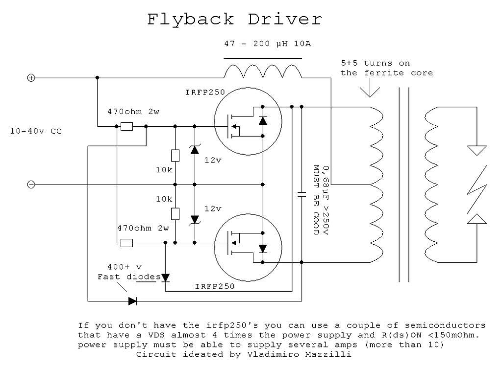
So I am making a simple ZVS circuit and I think I understand how it works, but I have a few questions such as, what purpose does the inductor play in this circuit? Are the zener diodes necessary or can they be replaced with normal fast switching diodes? Lastly is there a way to slowly (turn on the driver) so it doesn't consume so much current at turn on putting the circuit in danger?
Thank you,
Ben
1614908524696.png
 
The zeners need to be zeners. They are there to prevent the gate-source voltage from getting high enough to kill the mosfets.
 
what purpose does the inductor play in this circuit? Are the zener diodes necessary or can they be replaced with normal fast switching diodes?

Basically that general design that people keep replicating is just a really nasty circuit. It's only positive point is that it is simple.

At each half cycle of the oscillation, both FETs are turned on for a short time, creating a current spike.
And inductor can be thought of as a bit like a flywheel for current, it cannot change quickly so the momentary near-short-circuit does not destroy the transistors.

That use is what I'd class as a "Commutation choke".

You cannot turn it on slowly, as both transistors will start to turn on from the bias supply and may cook themselves before it starts to oscillate; the sudden turn-on and fractional imbalances in the circuit are what start the oscillator.

A separate non-overlap gate drive oscillator would solve many problems, but it adds the problem that it must be separately tuned to the resonant frequency of the power coil and ideally track that, so the overall circuit become a lot more complex.
 
1614928176789.png

 
View attachment 130107
That would be a possibility! Although his website is not in English the schematic should be enough. in his videos what is that weirdly shaped thing that appears to be attached to the primary? Also is that 13.7 Mega Farads?? Why do I need that much capacitance? Is L3 the secondary or are L1 and L2 just inductors to the primary?
 
miliFarads for smoothing, Higher current peaks,
L1 / C2 are for low pass filter
L2 C3 C4 for serial resonance
L2 primary
L3 secondary

I dont know what do you mean, can you make snap?
Ok thanks. Here a screenshot it’s sitting right above the mosfet
Why have I never seen milafarad before? Only Farad, micro farad, nano farad, and pico farad.
 

Attachments

  • FE27A552-2296-46AD-9FEA-062D1552CD49.png
    FE27A552-2296-46AD-9FEA-062D1552CD49.png
    2.2 MB · Views: 262
Last edited:
Ok thanks. Here a screenshot it’s sitting right above the mosfet
Why have I never seen milafarad before? Only Farad, micro farad, nano farad, and pico farad.
1614963903921.png

I think it is an insulator. I read that in comment section at YT if i am remember corectly
 
Why have I never seen milafarad before?
MilliFarad; like millimetre, 1/1000th
So 1000 uF

It's still not all that common, as at one time some places were wrongly abbreviating MicroFarads to mf, rather than using the "u" prefix for micro.

I reckon that ceramic ite you circles is some kind of high voltage capacitor, by the way - it appears to have a metallised surface plus an internal connection?
makes sense. I used to call uf “ultra farads” until an 8th grader corrected me XD
 
Last edited:
MilliFarad; like millimetre, 1/1000th
So 1000 uF

It's still not all that common, as at one time some places were wrongly abbreviating MicroFarads to mf, rather than using the "u" prefix for micro.

I reckon that ceramic ite you circles is some kind of high voltage capacitor, by the way - it appears to have a metallised surface plus an internal connection?
Makes sense. It was different project than.
K15U-1 | eBay
KVI-3 | eBay
 
Our cables at houses contains phase, neutral (working ground) and protective conductor PE (protective ground)
Bad translated sorry.
Its just ground.

P - protective
E - earthing
N - neutral
 
so the GRD above is neutral or wording ground?
and just to make sure, PE protective earth is like radio frequency ground like for a Tesla coil‘s secondary?
 
Ground is neutral / working conductor.
PE is conductor for RCD or FI.
Rcd is residual current device.
 
Why are there two capacitors in parallel? Are the ratings 6.8 nano farads? If so then can I just replace them with one 13.6nf cap?
1615066438441.png
 
Did you notice the little plus sign next to the 13,7mF "C1" one? That means it is an electrolytic cap, the other one is probably a ceramic. They each do something different to the circuit.
 
Status
Not open for further replies.

Latest threads

New Articles From Microcontroller Tips

Back
Top