Continue to Site

Welcome to our site!

Electro Tech is an online community (with over 170,000 members) who enjoy talking about and building electronic circuits, projects and gadgets. To participate you need to register. Registration is free. Click here to register now.

  • Welcome to our site! Electro Tech is an online community (with over 170,000 members) who enjoy talking about and building electronic circuits, projects and gadgets. To participate you need to register. Registration is free. Click here to register now.

Zero Crossing Detector inside the PIC16F18856 microcontroller

Status
Not open for further replies.

Flyback

Well-Known Member
Hello,

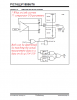
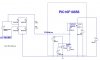
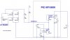
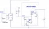
Please can you confirm that the Zero Cross Detector inside the PIC16F18856 can only work with a mains input (as in the attached schematic and LTspice simulation) if there is also a resistor to ground from the ZCDxIN pin? (R5 in the attached schematic).
If the resistor to ground is absent, then the current source internal to the PIC16F18856 will not operate, and therefore zero cross will not be detected….-[Both current source and current sink inside the micro must operate (alternately) in order for zero cross detection to happen].

Section 21.2 of page 316 of the PIC16F18856 datasheet makes it clear that the zero cross detection needs both the internal current source, and also the internal current sink, inside the micro, to operate alternately. If one never operates then there will be no zero cross detection.
As such, the resistor to ground (R5 in the attached schematic, is necessary for zero cross detection).
Do you agree?

The schematic in the PIC16F18856 datasheet shows a situation where the AC source and the microcontroller are both referenced to the same “ground”. But with the AC Mains setup of the attached schematic and simulation, this situation is not prevalent…and therefore the resistor to ground is needed (ie from ZCDxIN pin to ground)…do you agree?

PIC16F18856 datasheet:
**broken link removed**


If the current source doesnt get activated, then the OUT bit of the ZXDxCON register never gets cleared, and thus zero cross would never be detected. Therefore R5 is needed in the top post schematic.
The problem is, the datasheet doesnt say what current has to flow from the internal current source, or to the internal current sink, in order for current flow to be acknowledged by the micro.
That is, the PIC18F18856 datasheet doesnt tell what is the detection threshold of current. Do you know?

Even microchips app note on this, fails to say what is the current detection threshold...
https://ww1.microchip.com/downloads/en/AppNotes/90003138A.pdf
 

Attachments

  • ZCD on PIC16F18856.asc
    3.6 KB · Views: 187
  • ZCD in PIC16F18856.jpg
    ZCD in PIC16F18856.jpg
    69.4 KB · Views: 255
Last edited:
? it's likely the V.peak.min >= V.peak.max/6 and 300,700 µA maximums reveal some about the input sensitivity range not the I/O delay not the OUTP slew rate nor futher propagation delays to (evt1.) interrupts/statuses detected (evt2.) triggered/set when read

. . . since the "VCPINV, which is typically 0.75V above ground." is near to a digital-/signal ground e.g. NEG. rail for comparator . . . then it might be wise to reference your input signal to that very rail also . . . PS! if your bridge diodes are homogenous then the ~AC (bridge input-) Zero matches the DC (bridge output-) zero that perhps are the same as internal to PIC a half supply e.g. (Vdd - Vss)/2 - as it may also be possible that all these 3 (Zeros) are different and more over each a different function of time . . . e.c. , e.c.

. . . you re-level/-reference one of your inputs to (Vss or) VCPINV and Δ(V.L , V.N) to ZCD/RB0
using a level translator from https://www.electronicdesign.com/po...nal-amplifiers-and-instrumentation-amplifiers
the pg.622 has TABLE 37-17: ZERO CROSS DETECT (ZCD) SPECIFICATIONS by what the 300:300µA suggests the comparator OUTP is "0" at "no input" coz RB0 = half-supply as i get it
 

Attachments

  • dsxt.png
    dsxt.png
    23.8 KB · Views: 211
  • AC-Dummy-S1A.png
    AC-Dummy-S1A.png
    66.9 KB · Views: 210
  • AC-Dummy-S1A.asc
    7.9 KB · Views: 187
Last edited:
Thanks, but i believe the microchip zero crossing detector is not suitable for detecting AC mains zero cross....for these reasons...

We are trying to do Zero Cross detection with the PIC16F18856. The schematic and LTspice sim of what we are doing is as attached.

OUT bit:
Section 21.2, page 316 of the PIC16F18856 datasheet clearly states that zero cross detection is gotten from the setting and clearing of the OUT bit. Section 21.2 states that the OUT bit is set when the current sink is active, and cleared when the current source is active. The problem is that it doesn’t say at what current threshold the sink/source is considered to be “active”.

Square wave:
If the waveform being checked for zero cross is a square wave, then the zero cross circuitry is obviously going to work. If a square wave, then the OUT bit is obviously going to set/clear right at the zero crossing. However, if its a sine wave, then we don’t know where on the rising sine wave the current is going to be great enough for the source or sink to be regarded as “active”. As such, we cant work out where exactly will be the zero crossing.

Detecting zero current:
We could pretend to ourselves that the micro will faithfully detect the exact zero of current. However, if it was capable of doing this, then why does it need the peak of the current to be 300uA? Also, concerning section 21.6, page 318 of the PIC16F18856 datasheet, why, if it is capable of detecting zero current, does it need the peak current to be at least 100uA high?
Does this mean that for the detection of current in the current sink or source, at least 100uA of current flow is needed? –If not, then why is there this 100uA minimum figure?

If the micro can detect the zero of current, then being sensitive to that low level of current would mean that it could easily be messed up by noise…chattering of the OUT bit. Microchip’s TB3138 document recommends a capacitor at the ZCDxIN pin to mitigate noise, but the datasheet makes no mention of this.

So if the ZCD circuitry in the micro can really detect zero current, then is it sub 1uA that it detects as zero Amps?, or sub 2uA?, …or sub 3uA……?.....And if it really is sensitive enough to be able to detect these low levels, then it would be very easily triggered by noise…specially with a signal originating from the mains like in our case.

Sine waves:
This is all relevant for sine waves, because if the detection of current is at some point above zero amps, then how far above zero amps is the detection threshold?.....because with a sine wave, if the current detection point is relatively high, then the OUT bit setting/clearing may well be a significant time interval away from the zero crossing…..and so we will not be accurately pinpointing the zero crossing. All this confusion never arises with bipolar square wave zero crossing…because a square wave immediately rises to its peak at the zero crossing. It is my impression that the ZCD circuit in the PIC16F18856 was designed for bipolar square waves. The datasheet fails to elucidate on the required parameters needed to properly use this ZCD circuit with sine waves. We actually have a microcontroller with nothing more than an “RSERIES” resistor connecting to the ZCDxIN pin and use it with sine waves as in the attached schematic. (ltspice simulation also included). The circuit appears to be working. However, it may be just that we’ve been lucky. –Maybe we have been narrowly operating at the edge of a “tolerance cliff” and are just lucky to not have gone over it……maybe with a different batch of microcontrollers we would not be so lucky, as maybe they would not be able to so closely detect the zero current point. As you can see, our current circuit is interfaced to the mains which is at the other side of a bridge rectifier, so for us, the current source barely operates at all….(it only sources some 2uA). According to section 21.2, page 316 of the PIC16F18556 datasheet, the OUT bit needs the current source to operate in order to be able to get cleared. For our situation, the ZCD circuitry would need to be able to detect 2uA of current flow in order to be able to clear the OUT bit. –Maybe the batchs of microcontrollers that we have so far used have been able to do this, but it is obviously going to be suspected that other batches will not be able to do this….and so we are running the risk that the ZCD circuit will not work.

Contradiction 1:
Another problem is that Microchip’s “Technical Brief” document (TB3138) contradicts the ZCD section of the PIC16F18856 datasheet. TB3138, on page 1, states that the peak current that can be sourced/sinked is 300uA. Wheras the PIC16F18556 datasheet states that this figure is 600uA. Which is it? We need to know because our mains varies from 210VAC to 265VAC, and we need to be sure that at high mains we don’t go above the maximum allowable current.

Contradiction 2:
Also, there is another contradiction…… the datasheet specifically states that it is current flow from the source that clears the OUT bit, and current flow into the sink that sets the OUT bit.
However, TB3138, on page 6, specifically states that the OUT bit changes state when the current into the ZCDxIN pin is zero….Current into the ZXDxIN pin can become zero if only one of the current source or current sink operates. This is a contradiction. According to the TB3138, only the current source or the sink need to be monitored..not both. –This is not in accordance with the datasheet.

Sine wave reference point:
All of the discussion in the datasheet and the TB3138 document concerns detection of zero cross in sine waves that are referenced to the same ground as the microcontroller. In such a case, the current source and sink would obviously alternately operate….and provide similar waveforms in the current source/sink. This is not our application case, because our microcontroller is not referenced to the same ground as the mains, and the mains is at the other side of the diode bridge. The datasheet/TB3138 document makes no mention of our application case.

I don’t think we can be sure of reliable operation of the ZCD circuitry in the micro, and therefore believe we should revert to using a anti-parallel diode optocoupler circuit instead.

The attached simulation shows our application case in the LTspice simulator.

(please note i believe microchip are usually the best at explaining tech points)

TB3138 app note on ZCD
https://ww1.microchip.com/downloads/en/AppNotes/90003138A.pdf

PIC16F18856 datasheet (page 314- discusses ZCD)
https://ww1.microchip.com/downloads/en/DeviceDoc/40001824B.pdf
 

Attachments

  • ZCD on PIC16F18856.asc
    3.2 KB · Views: 187
  • ZCD schematic.jpg
    ZCD schematic.jpg
    67.1 KB · Views: 218
Fig 21.2 on page 315 of the PIC16F18856 datasheet shows optional externally attached pull-up and pull-down resistors.
Please can you confirm that in our setup, with AC mains, the pullup resistor (pulling up to Vdd) would never be needed?
This is because the pullup resistor would simply bring the current source into action, and that would be pointless, because the high-going half cycle of the AC mains will already have brought the current source into action (the “current source” being the current source inside the PIC16f18856).

Schematic and LTspice simulation of our setup is as attached.


PIC16F18856 datasheet:
https://ww1.microchip.com/downloads/en/DeviceDoc/40001824B.pdf
 

Attachments

  • ZCD on PIC16F18856.asc
    3.4 KB · Views: 207
  • ZCD schematic.jpg
    ZCD schematic.jpg
    70.5 KB · Views: 210
Status
Not open for further replies.

Latest threads

New Articles From Microcontroller Tips

Back
Top