Hi,
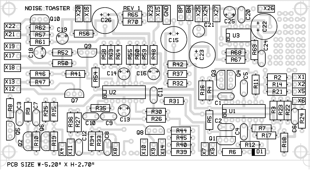
I soldered together the Noise Toaster

 musicfromouterspace.com
most of it is working. some of it, like the white noise generator, is not working, so Im troubleshooting it.
I went back through the instructions and diagrams and read the section below, which I didnt remember reading before:
"double sided PCBs have plated through-holes, which are often used to route circuit connections between the top and bottom sides of the board. These top-to-bottom circuit connections are called vias. All pads on the board not used for component leads must be drilled and have a 'Z' wire inserted and soldered. A 'Z' wire is a piece of solid 22 or 24 gauge hookup wire that is inserted through the pad's hole and then bent at a 90-degree angle on the top and bottom sides of the PCB. Trim any excess wire after bending, make sure the ends are not shorting to adjacent pads, and then solder the 'Z' wire top and bottom."
First, why would there be vias that wouldnt be used for component leads on the board? If the board was professionally manufactured, wouldnt all vias be used for component leads?
Next, what is the purpose of the 'Z' wire? It seems like it's supposed to continue the flow of electricity from the top of the board to the bottom or vice versa, but the way it's described in the instructions is confusing. It seems like that the 'Z' wire should be connecting two pads.
Last, since the PCB is professionally manufactured, wouldnt all of the vias already be connected with the top and bottom copper layers?
I searched online for other people talking about 'z' wires but I havent found anything.

I soldered together the Noise Toaster

Music From Outer Space Your Synth-DIY Headquarters
Music From Outer Space is your synth-diy headquarters. Analog synthesizer plans and schematics.
 musicfromouterspace.com
most of it is working. some of it, like the white noise generator, is not working, so Im troubleshooting it.
I went back through the instructions and diagrams and read the section below, which I didnt remember reading before:
"double sided PCBs have plated through-holes, which are often used to route circuit connections between the top and bottom sides of the board. These top-to-bottom circuit connections are called vias. All pads on the board not used for component leads must be drilled and have a 'Z' wire inserted and soldered. A 'Z' wire is a piece of solid 22 or 24 gauge hookup wire that is inserted through the pad's hole and then bent at a 90-degree angle on the top and bottom sides of the PCB. Trim any excess wire after bending, make sure the ends are not shorting to adjacent pads, and then solder the 'Z' wire top and bottom."
First, why would there be vias that wouldnt be used for component leads on the board? If the board was professionally manufactured, wouldnt all vias be used for component leads?
Next, what is the purpose of the 'Z' wire? It seems like it's supposed to continue the flow of electricity from the top of the board to the bottom or vice versa, but the way it's described in the instructions is confusing. It seems like that the 'Z' wire should be connecting two pads.
Last, since the PCB is professionally manufactured, wouldnt all of the vias already be connected with the top and bottom copper layers?
I searched online for other people talking about 'z' wires but I havent found anything.
