Continue to Site

Welcome to our site!

Electro Tech is an online community (with over 170,000 members) who enjoy talking about and building electronic circuits, projects and gadgets. To participate you need to register. Registration is free. Click here to register now.

  • Welcome to our site! Electro Tech is an online community (with over 170,000 members) who enjoy talking about and building electronic circuits, projects and gadgets. To participate you need to register. Registration is free. Click here to register now.

What's the purpose of connecting this collector to power?

Status
Not open for further replies.

BobbyHood

New Member
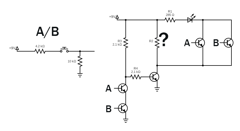
I'm watching Ben Eater's logic gate video and trying to figure out his XOR gate. This is basically what he did. I don't understand why the path exists where R2 is located (next to the question mark). Why would you connect that collector to power? It seems like it would just waste power when it's not being used.

Logic Gate - XOR.png


Video:
 
When the transistor connected to R2 is turned on, there is no added value in having R2 in circuit.
But when that transistor is turned off, R2 pulls the emitters of the two parallel transistors up to 5v, which is far better than having them floating.

JimB
 
When the transistor connected to R2 is turned on, there is no added value in having R2 in circuit.
But when that transistor is turned off, R2 pulls the emitters of the two parallel transistors up to 5v, which is far better than having them floating.

JimB

Ok, I've been trying to understand this "floating" thing. In this case we're pulling it "up" to equalize the voltage so there isn't a kind of "hanging tension" between the collector and emitter. Is that right? And in the case of a floating base, we pull it "down" because we don't want it inadvertently opening the transistor. So floating just means the value isn't explicitly set, which allows it to do whatever it wants when there's EMI or cosmic rays or gremlins or whatever. Sorry if that's confusing, I don't have the vocabulary for this stuff yet.
 
Think of it as an inverter, when the base is powered (A or B off) the collector is at 0V. When the base isn't powered it's at 9V via the resistor.

Mike.
 
Nobody is looking at the videos, so the answers are based on miss-information.

The circuits shown are logic gates. Therefore A and B (both As and Bs in this case) are connected to logic 0 (low) or logic 1 (high). The schematic doesn't show these connections but the truth table to the left does. These inputs aren't floating – they are either high or low.

The video also seems to explain exactly what's happening pretty clearly.
 
Ha I'm still confused. The reason is because the circuit continues to work if I just disconnect that path. In fact it works better, because A and B then give me a more equal 3V across the LED. The way it's designed, A gives me 3V and B only gives me 2.7V. You can see this in the video too. One button shows a dimmer light.
 
  • Like
Reactions: Buk
The reason is because the circuit continues to work if I just disconnect that path. In fact it works better, because A and B then give me a more equal 3V across the LED.
That's because it is a very crude, primitive circuit, purely to demonstrate basic logic principles - not good electronic design practices.

Practical circuits have to stand less than perfect components - and have their inputs and outputs using compatible signal levels, so they can be cascaded for more complex functions.

These are real-world transistor logic circuit examples:

A DTL (Diode-Transistor Logic) triple NOR gate from a 1960s computer:
And the actual thing, a small plug-in board:

And the internal circuit of a TTL (Transistor-Transistor Logic) XOR gate, each section of a 7486 IC:
 
As you can see when one input is 0 its irrelevant what the other input is doing -

1628766919735.png


Regards, Dana.
 
As you can see when one input is 0 its irrelevant what the other input is doing
Logic-wise, yes.

However, that again is an over-simplified diagram and not a real world one.

So - voltage-wise and in practice; no!

If a CMOS input is near mid supply, both the upper and lower transistor it feeds can turn on at the same time. That can cause excess current or possibly oscillation.

Most logic ICs have signal buffers before splitting the signal to different points internally.

eg. The real internal arrangement of a 4081B AND gate is detailed below; each input directly drives a Complementary pair of MOSFETS.
[The CMOS name comes from the Complementary MOS construction]

The minimum "high" and maximum "low" voltage levels are given in datasheets. Leaving an input in between these levels, near mid supply, is a "real bad thing".. Another application of the "Nothing floating" rule.

main-qimg-4735e8bde0d4363f4e91728d097b4aab


The exception is with devices that have schmitt trigger inputs - they can have any voltage within the supply range, but only "switch" when it's above the high threshold or below the low threshold.
Good for debounce, timing circuits, oscillators etc.
See eg. 40106 and 4093 for CMOS examples of those.

Would it be true if Tr, Tf << Tpd then the simple diagram still holds ? Which
is "normally" what ones wants in design.

Not an expert here by any means.


Regards, Dana.
 
Would it be true if Tr, Tf << Tpd then the simple diagram still holds ?
As long as it's another logic output with appropriate levels, or some reasonably "fast" signal, it should work fine.

My answers are based on the OPs query about internal voltages in a gate circuit and how the circuits work, rather than just the intended logic results.

More info on floating or slow input changes:
 
Status
Not open for further replies.

Latest threads

New Articles From Microcontroller Tips

Back
Top