Continue to Site

Welcome to our site!

Electro Tech is an online community (with over 170,000 members) who enjoy talking about and building electronic circuits, projects and gadgets. To participate you need to register. Registration is free. Click here to register now.

  • Welcome to our site! Electro Tech is an online community (with over 170,000 members) who enjoy talking about and building electronic circuits, projects and gadgets. To participate you need to register. Registration is free. Click here to register now.

Using MMIC RF chip

Status
Not open for further replies.

Swanepoel

New Member
Hi all,

Having played around with my new DVBT dongle I kind of like the idea of decoding ADSB signals. This is all fine and well but since I am not that close to an airport I see limited traffic. So the next logical step would be to get a LNA between my antenna and dongle, the not so logical step is me trying to build my own LNA or even just a RF amplifier (when there are cheaper ones to buy online). But I wanted to learn more about RF circuits, so why not give it a shot. After looking around it seemed not that hard to do, I just have to buy a MMIC amplifier, some capacitors, an inductor and then solder them to a pcb!
So I selected the ADL5545 30MHz to 6GHz gain block amplifier and skipped to the section where they show the basic configuration in the datasheet and also bought the recommended capacitors and inductors. To power the amplifier I bought a LM340 5V regulator that I solder to the same board.

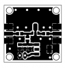
For the PCB I figured I should be more careful since this is UHF and kept the board small (30mm x 30mm) and double sided with the bottom as ground. I wanted to make sure the input and output traces where balanced 50 ohm transmission lines but then read an article which stated that if the tracks are shorter than 1/10th of the wavelength then its not needed. So then I skipped that thought. Then the topic of via's and via fences also popped up and I made a few 1mm (the smallest drill I have) via's around the board.

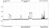
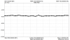
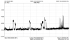
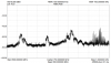
So I made the PCB and carefully soldered the SMD parts to it. As a first test I powered the circuit up and tested for 5V on the regulator output, which was fine. Then I connected the amplifier to the antenna and my dongle and powered it up! The whole noise floor just jumps up by about 30dB drowning out any signals that where there before!

So since then I have been troubleshooting what I could have done wrong and how I can fix my amplifier but no luck!
Have I completely underestimated the difficulty grade of building such a circuit?
Is there any rookie mistakes that I could have made or any advice for maybe a future attempts?
Any advice on how I can troubleshoot these kind of circuits?

The schematic is pretty basic and just a copy of the one in the ADL5545 datasheet with the added LM340 regulator, so I will add the top layer of my circuit if it helps.

Thanks for your time guys...
 

Attachments

  • AmpTopLayout.png
    AmpTopLayout.png
    6.8 KB · Views: 298
Sounds about right. Your amp is doing what is expected, amplifying about ~25 dB. Your Amp is very broadband and is just amplifying everything, ambient noise included. Your choice of Amp for this case was probably not ideal as it's NF (Noise Figure) is not optimal for a LNA. Typical NF value for a LNA (Low Noise Amp) would be something on the order of <2 dB, your amp is greater than >3 dB, and that figure is based on optimal board layout.
What will contribute noise to your amp NF is power dissipation, and looking at your layout, you should have added more copper surface for the amp to dissipate power. That is to say, added more via's to bottom ground plane around the amp. Looking at the Amp Data sheet NF goes up about a dB with a 60 deg C rise in device temp.
BW (bandwidth) of the front end also effects NF, you can improve NF by limiting your BW to the frequency region of interest. Perhaps on off the shelf 900 MHz LPF (low pass filter) with SMA connectors, but that is pricey and probably not worth it. Your best bet if you want an LNA is to use a LNA part with a NF <2 dB. The part you selected is more of a general purpose amp most likely used in the IF gain stage. You might want to do a google on cascaded Noise figure. From the Friis equation one can deduce the first stage NF will set the overall system NF, so first stage AMP NF is critical for discerning low signals.

adl5545specs.PNG
 
It is not appropriate that your entire noise floor pops up about 30 dB unless it the noise is being received by the antenna (ie. all from the environment). So, one test to do first is to operate the amplifier without an antenna and see if that noise still jumps up. Can you attach a 50 ohm source or resistor to the input somehow? This would terminate the input correctly and eliminate any environmental noise. If you still get 30dB more noise after doing this, then there is something wrong. One thing that could be happening is that your amplifier is oscillating. This can easily happen when you have a lot of gain, which you do, and when you have a broadband circuit, which you do. Remember that with a broadband amplifier, you have to treat your layout, your tuning and your bias circuits as if you are building an amplifier at the highest frequency at which the device still has good gain. That is in excess of 6GHz. Your pcb layout and construction have to work at that frequency in order to keep the amplifier stable. Your layout does not do this very well, at least for frequencies above about 1.5 GHz. You can change the amplifier to have relatively narrow bandwidth. This can sometimes be done by putting a bias circuit on to the output that provides a reasonable load at the frequency you want, but a very poor load (ie. very low impedance) at higher frequencies, thus killing the gain at higher frequencies. Perhaps a small shunt capacitor on the output would be helpful in this way.

An amplifier that is oscillating at some frequency away from your frequency of interest is usually quite noisy. That is one clue. Depending on the bias arrangement, it may also be drawing more DC power than it should, so make a measurement of your DC current into the amp. If the current is normal (ie. per the data sheet) don't rule out oscillation, but if the current is significantly higher or lower than expected, then this may be a good indicator of oscillation.

Your layout could be improved by having some sort of grounding via connection directly under the amplifier component, but I see that this would be almost impossible for you, and you do indeed have a grounding via fairly close, so not sure how useful the advice is. however, the degree to which you have tied the top layer ground plane to the bottom one is very different between your layout and what I would do (and what is shown in the data sheet) for a broadband amplifier like this one. Better grounding may be in order. One thing you can do is connect top and bottom ground around all the edges using copper tape seam soldered all the way round.

another thought: if the noise goes away when you remove the antenna, as mentioned above, you should also try a different antenna. It is possible that the antenna impedance is too reactive at some frequency that the amp doesn't like and is stimulating it to oscillate. Admittedly this doesn't happen all that often, but it is possible.
 
Last edited:
Hi Guys,

Thanks for the huge amount of insight, help, advice and explaining but I am still a bit lost. I have done another couple of tests tonight (this time using a better spectrum analyzer) and will attach the results. For the first test I sweeped (averaged to better see the noise floor) the spectrum between 500MHz and 1GHz and could see some DTT (Digital Television) channels peaking some 20db or more above the noise floor. Then I inserted my amplifier in between and again performed the sweep. On the sweep with the amplifier I should for sure see some of those channels right?

My understanding is as such: say my gain is 25dB and my noise figure 6dB then after inserting the amplifier the noise floor should rise by 25dB + 6dB = 31dB. The signals should then show up 25dB above noise and my S/N reduced by 6dB right? But I am just seeing the increased noise floor and no signals.

I then tried with and without an antenna connected and it seems to make no difference, the noise floor still jumps up about 30dB. Not sure if it means anything but having the amp inline and not powered I can see some of the DTT signals on the spectrum at a reduced level, probably just passing through. Also then tried with a 50 ohm resistor on the input but the result stayed the same. So I guess it looks like the amp is then oscillating... My multimeter shows about 45mA current draw when the amp is running, which is a bit lower than the 56mA specified.

Tomorrow I will try to solder the top and bottom ground planes together and try again.

I was thinking since I already built this amp it would be great to know if it is at least working and if not, it would be an interesting learning experience to solve it.
 

Attachments

  • NoAmp.png
    NoAmp.png
    51 KB · Views: 284
  • WithAmp.png
    WithAmp.png
    32.7 KB · Views: 281
I agree that your sweep "withamp.png" doesn't look right. Oscillation is one possibility, but not the only one. Now that you have a bit better spectrum analysis capability, can you use that to look around in frequency for a really big spurious output from your amp?
I did a quick back-of-the-envelope calculation of the total output power of your amp. Its a bit eye-opening. If we assume that this spectrum that you show continues pretty much flat like that down to about 100MHz and perhaps up to 2GHz, then integrate the total power:
=indicated power + 10log (total spectrum/resbw) = -57 dBm+(10 log(1.9e9/100,000)=-14 dBm. This may well be the limit of the output power of your amp, and it could be more if your noise spectrum continues to 4GHz. That's a lot of noise. If the amp is limiting, this could explain why you don't see any signals. Why is it limiting? Yeah, i still suspect oscillation (or general instability, which is much like oscillation only it isn't on just one frequency. In the case of a very messy unstable behavior, you can get an output spectrum that is so full of various oscillations intermodding with each other that the output spectrum becomes a great big broadband mess).

I think you need to move around a bit in frequency and see what you can learn about the spectrum of that "withamp" situation.
 
Last edited:
Wow, that is not what I was picturing in my head, actually not sure what I was thinking. I think Ron is correct and that you got an issue somewhere.

My understanding is as such: say my gain is 25dB and my noise figure 6dB then after inserting the amplifier the noise floor should rise by 25dB + 6dB = 31dB. The signals should then show up 25dB above noise and my S/N reduced by 6dB right? But I am just seeing the increased noise floor and no signals.
No, this is not quite correct.
See the Friis Formula for cascaded NF.

ea52aeef02e200e033d18a71646dd047fc7baf8c

7b304d432e53cda2f69964e2cf0a0086d324ba85

As I had mentioned in my earlier post, the overall NF is pretty much dictated by the first stage, but you have something else going on and your in good hands with Ron.
 
Mike makes a good point, and this bears a bit further discussion. Your spectrum analyzer is a receiver with, very likely, an extremely poor noise figure. My old HP 8593E has a noise figure of about 25 to 35 dB (depending on whether I let the input attenuator stay on auto or not). Newer analyzers may have much better NF, but we should not assume yours does. In your first measurement (NoAmp.png) the noise floor appears to be around -95 dBm. If we assume that this is not environmental noise, this means your analyzer has a noise figure of about 30 dB (noise floor is the sum of KTBR in 1Hz which is -176 dBm plus a bandwidth correction of 50 dB to account for your res bw 100KHz, plus the noise figure of the system). By applying the formula for cascaded NF, the total NF of the system made up of your experimental LNA attached to the spectrum analyzer becomes 8.5 dB and this is referenced to the input of the system. This means that if your amp is working properly, what you should see in "withamp" is a noise floor at about -92.5 dBm and a signal (let's use the one at 800 MHz) of around -40 dB, so the SNR would have improved by a whole lot by adding an LNA. This is because you will have improved the noise figure of your receiver system by 21 dB.

The overall noise figure is only dictated by the first stage when the first stage gain is somewhat greater than the follow-on noise figure. In this case, it isn't , so we don't get down to 6 dB, only down to 8.5 dB. If you are checking my figures, remember that the F and G values in the equation are not dB values, they are Noise Factor and Power Gain in linear terms, not dB.

To check all this, I set up a broadband amplifier with 32 dB gain in front of my spectrum analyzer (also with 100KHz RBW). With input signal set to -60 dBm, I see a noise floor of -98 dbm and a signal of -60 dBm on the screen. Then when I add the external amplifier, my signal goes up to -28 dbm while my noise floor only goes up to -92 dbm.


In addition to scanning around the spectrum with your spectrum analyzer, there are some other things I suggest you do to gather clues. Another one is to take a small value ceramic capacitor (one with wire leads), say about 47 pF or so, in your fingers, and shunt the output of the amp to ground with this cap and just watch what the noisy output does. You have to be a bit careful, but just touch the wire leads to ground and to the hot point for a moment while watching your analyzer. You can put this cap first at the output to ground, then at the input to ground, and at any point in the DC bias circuit as well. If nothing happens, no harm done. But if you see the noise drop dramatically, then maybe we have a clue. For this to be helpful, the wire leads on the capacitor should be short, say about 5 mm long.\

Another possibility is that your voltage regulator is unstable. This family LM340/LM7805 is not one that I would suspect of instability, but I see that you have no input cap on the regulator. Perhaps try putting a good size cap there, like a 0.22uF ceramic.
 
Last edited:
I was just looking at your layout again, and noticed that you have an opening in the ground plane around the ground tab (heatsink tab) of the amplifier. I don't like that. You should allow the ground plane to flood over onto the pad for the tab. Can you put some copper tape or something to bridge that gap?
 
Hi Ron,

That last comment of yours was right on the money!
I flooded the amp's ground terminal across the gap unto the PCB ground and tried again. Things dramatically improved! Although not perfect I could now see peaks on the spectrum representing the DTT signals. Then I picked the board up and while holding it in my fingers (closer to the output side) things cleared up even more to a pretty good level! Its alive! I will attach some pictures. Thanks a lot guys, for taking the time and helping me solve this!
Thinking about it, flooding the ground terminal not only made it work but would also allow better heat dissipation and as Mike mentioned this will then reduce the noise figure with temperature increase.
So I guess my fingers is just grounding it better and now I just need to improve the grounding, I have not yet made the grounding seem on the outer edges as you mentioned earlier. Will do that next to see if I can get it to always perform the same as when I am holding it in my fingers.

Getting back to the calculations I checked the spectrum analyzer (Signal Hound BB60A) and it seems that I have a dynamic range of about 75dB. The second set of sweeps I performed with the reference level at 0dBm, since with the -20dBm level the noise floor and signals seemed distorted when running the amp. I guess this is probably due to over-driving the front-end a little bit. This makes it little harder to see the increase in noise floor but using the first signal at around 570MHz I see levels of about -73dBm before using the amp and -53dBm with the amp so getting about 20dB gain right?

This is real interesting stuff and takes some time to sink in. So what you are also saying is that on its own the spectrum analyzer has a pretty bad NF. But when I add the LNA then the LNA is the first device in the system and like you and Mike mentioned, it contributes to the largest part of the system NF. This then has a huge impact and lowers the system NF and also increases my signal to noise far beyond what the spectrum analyzer was capable of doing on its own?
 

Attachments

  • WithAmpHoldingInHand.png
    WithAmpHoldingInHand.png
    68.1 KB · Views: 285
  • withAmpGNDPadSoldered.png
    withAmpGNDPadSoldered.png
    70.5 KB · Views: 279
I remember how difficult it was, when I first started out in RF design, to learn how to debug a board whose behavior changed depending on how you held it with your fingers. Been there, done that. Its all about stability. Your board is what we call "hot", meaning that the amplifier return currents, those supporting the output transmission line to the load, and those traveling from the bypass caps to the ground terminal of the amplifier, for example, have too far to travel. You can call it grounding if you like, but think of the current loops that want to flow on the board and you begin to see the paths they must follow. The grounds that support flow of power on the output trace must connect back to the amplifier ground terminals with the lowest possible inductance and shortest path in order for the amp to work its best. In your board, imagine current flowing from the ground side of the bypass capacitors wanting to go back to the amplifier. They have to travel a tortuous path the long way around and through some skinny bits of copper to get where they want to go. The layout would have been better if the cold side of those caps was directly connected via wide plane to the amplifier ground pin. Commercial product designers face this kind of problem all the time because its hard to stuff in all the parts you need, but they have the advantage of plated-through vias in the ground plane, which do an excellent job of shortening the current path back to the amp. It isn't clear how to fix things on your board, but one way would be to somehow turn the bypass caps around and connect them to ground directly beside the amp ground terminal. Gotta do this with low inductance methods too, so copper tape rather than skinny wire is called for. Start by moving only the smallest value capacitor as that is likely the one most involved at the highest frequency, at which the current paths look the longest.

Putting copper tape on the edge of the board is probably going to help a bit. Adding some more ground vias would help if you could do that in a few spots near where the currents are flowing the strongest. Remember that ground currents want to flow on the path of lowest impedance. In the case of the output transmission line, this means directly underneath the output trace on the inside surface of your ground plane layer. How does the current on the inside surface of the plane below the output trace find its way back to the ground terminal of the amp? We usually help this process by putting ground vias near the ground terminal of the amp. The current will flow where it can, so the fields will transition from directly between the trace and ground, to being somewhat planar on the top layer, meaning that the current will move to the top layer ground plane through electric and magnetic field coupling in order to get to the amp terminal. This just happens automatically because that is the only path the energy can take. But there is an impedance involved that must be overcome and that is a compromise that we have to minimize. This sort of mechanism becomes clearer if/when you use a 3d electromagnetic field simulator program to study how current flows into and out of an IC at very high frequencies. Maybe you'll get a chance to do that kind of study some day.

As for the ground currents returning from the bypass caps back to the IC, they would have had an easier time (ie. faced a lower Z) if there were ground vias at their cold terminals coupling current down to the ground plane so that they could find a low inductance path back to the amp. Copper tape on the edge of the board, which is nearby to the capacitors, should help a bit, but the current still has to get around your DC power connector to get to the edge of the board, too bad.

I wouldn't make such a fuss about ground currents if the amplifier only had gain up to 200 MHz or so, but this one has gain up to 4GHz and more, so gotta be fussy.
 
Last edited:
Hey Ron, let me run this by you. Refer to attached image below. One thing that I thought may be happening it that the Bias path may have some RF on it, consequently coupling back to the input via radiated path. What do ya think? One test may be to try and create a shield to block that path? But I defer to you :)

RFAMPpcb.PNG


My thinking here is that some RF energy from the output is on the bias path and the regulator lead may act like an antenna and provide a feedback path back to input. Depending on phase you may get oscillation.
May experiment with grounded shield between the path. Just a thought.
 
Last edited:
Hi Mike. While it is possible that a shield may help, it is a matter of degrees. In this case, both the bias node and the output transmission line should be relatively low impedance, making it harder for their fields to couple significant voltage or current. Especially the bias node, which should, theoretically have an impedance of less than one ohm. Imagine the thevenin equivalent circuit of coupling from the output trace back to this node. The source is a mildly leaky transmission line and I'm not sure what Z to assign to that leakage, but it might be significant, so I would say 100 ohms (wild guess). The coupling distance has an impedance that is mostly a function of distance and height of the terminals on the regulator and output coupling cap as these two points will have the lowest couplng Z. That will be somewhat high Z, maybe 1000 ohms (another wild guess, mainly for example) and probably is the Z of a capacitance of about 0.05 pF (my rough guess at the C across those terminals that rise above the plane of the board). The destination load Z at the bias node would be very low, as mentioned, so the voltage generated across that load (voltage divider: 1 ohm divided by 1101 ohms = -60 dB if my wild guesses are anywhere near correct) should be very small. Is its smaller than 25 dB (which is the loop gain)? Yeah, I think so. Of course, this depends on how well the bypass caps are doing their job, which may not be great at present. But I would re-position one of the bypass caps first to deal with this and if that fails, consider your idea of shielding. Shielding is hard to do and with a bit of copper stretched across that red arrow path, you will affect the electrostatic coupling, but not have as much of an effect on magnetic coupling unless you wrap the shield all way around the output circuit (to box it in), which is hard to do.

I've tried this in the past in a sort of similar scenario and actually made things worse, but that was when the board was housed in a metal box, which provided more funky feedback paths that this open board won't have. I've also tried using RF absorbing rubber gasket adhered directly to ground plane or inside of box, which helps in surprising ways because it increases the impedance to surface currents on an undesired feedback path.
 
Hi Ron and great response. I agree with and learned a few things as well with what you said. The shield was not mentioned as a solution, rather a diagnostic aid. That is to say, determine sources of instability such as unwanted feedback paths. I wonder if a 1-2 dB pad at the input would do anything?
 
Changing the caps sounded like a pretty hard task, it seems that there might be enough space to jump one of them (maybe the smallest one like you mentioned) over to the inside and much closer to the amp ground pin. But then the statement "They have to travel a tortuous path the long way around and through some skinny bits of copper to get where they want to go." seemed like an easier problem to solve, especially the "skinny bits of copper part". So I used a bit more solder on each capacitor to also flood that small gaps around the landing pads. I did the same with the SMA connectors on either side, flooding the small gaps around the pads.
I connected everything back up and now its running perfectly with almost no distortion and just the clean signals pushing strongly through the noise floor! Touching some parts of the PCB distorts the output but I guess this is normal, at least now I don't need to hold it in my fingers to make it work! Now I can start playing with my amplifier and try measuring its noise figure, exact gain, etc
Its amazing how sensitive PCB layout is when it comes to high frequency RF and I sure learned a lot! Feels like I want to print this thread with all the information you guys provided and file it for future use since I will for sure play with some more RF circuits. Thanks again Ron and Mike for all the help, on my own I would have thought the chip was fried and gave up a long time ago!

While we are on this interesting topic of PCB design for these small MMIC amplifiers. I spoke with one of the guys from work yesterday, he is very much into amateur radio and I told him about my amp project. Today he brought me a PCB from **broken link removed** What are your thoughts on this design? Can I use it as a reference design for future amplifiers? If I understood correctly this design also suffers from having the bias capacitor grounds pretty far from the amplifier ground pin...

If I may, I have also another question or maybe I should post it in a new thread. While having trouble getting my amplifier to work I went ahead and purchased one of those LNA4ALL amplifiers. So now that my amplifier is also working, would it be possible to cascade the two to get even more gain? I will for sure use the LNA4ALL as a first stage but my gut says this is not as easy and I would probably need a filter or something between the two amps?
 
The distance between those bias cap grounds and the amp package is a bit far for my taste, but it would be easy to hack a modification to put the 100pF capacitor in a more ideal position, so the pcb is still valuable. But if you are laying out a new board for professional fabrication, I would adjust the layout to improve the cap placement.

You can indeed cascade the two amps, but beware that adding more gain comes with a price, and that is the increased risk of intermod and other negative effects of limiting in the receiver. A filter is not absolutely necessary, but it could help to keep out strong signals well away from the frequencies that you want to receive, which in turn avoids intermod from those signals.
 
A good article explaining intermod, imd, ip3.

**broken link removed**

One thing about RF Amp design is that there is trade offs. Naturally we want our cake and to eat it to, but like most things this is never the case and RF amp design is no exception.
Having the best of both worlds is desirable in most things but like most things choices must be made. In RF amps noise figure (NF) sets a quiet output no hiss and allows discerning a weak signal more easily. See MDS. The Lower NF is the better. Now another parameter of concern is intermod as it is commonly called or oip3, ip3 are some other terms used. Intermod is undesirable because it will desensitize a receiver and further cause out of band signals to be in the final output.
Unfortunately to get good NF we want to run the amp with as low a current as possible as you know more current makes more heat which in turn more noise. But at same time we want high dynamic range distortion free for good intermod which usually implies high current for high dynamic range. So as you can see that is where a trade off must be made.
Does that make sense at all? Sorta hard to explain. I'm sure Ron can explain better. But what I said should give you basic idea why you should care about both intermod and NF.
 
I was just looking at your layout again, and noticed that you have an opening in the ground plane around the ground tab (heatsink tab) of the amplifier. I don't like that. You should allow the ground plane to flood over onto the pad for the tab. Can you put some copper tape or something to bridge that gap?

and he's done the same thing for the bypass caps and the input and output connectors

all a bad thing to do
 
. I wonder if a 1-2 dB pad at the input would do anything?
Hi Mike. I forgot to comment on this idea. I would avoid padding the input because that adds directly to noise figure. If your intention is to reduce gain, doing it at the output would be better, and doing it in a frequency selective way (ie. reduce gain above 1GHz but not so much below) would be even better. If your idea is simply to diagnoise feedback paths, it might be useful to put this anywhere to gain some clues (hey, I made a pun!), but it isn't simple. You would have to put down two or three resistors very tightly to the RF path and close to the amp package, so its physically tricky.
 
Status
Not open for further replies.

Latest threads

New Articles From Microcontroller Tips

Back
Top