Continue to Site

Welcome to our site!

Electro Tech is an online community (with over 170,000 members) who enjoy talking about and building electronic circuits, projects and gadgets. To participate you need to register. Registration is free. Click here to register now.

  • Welcome to our site! Electro Tech is an online community (with over 170,000 members) who enjoy talking about and building electronic circuits, projects and gadgets. To participate you need to register. Registration is free. Click here to register now.

Using LM324 and OP07 for controlling voltage

Status
Not open for further replies.
Hello there,

This post might be a fun for learning, some of you might laugh to see it once!
Trying to control old TCA785, a phase control IC, https://images.100y.com.tw/pdf_file/TCA785P.pdf.

But before that, take a look my circuit in this attachment ….
cry.gif


1. Lets say 0-10 VDC signal in increments of 1 volt or a 0-20 mA signal in increments of 1 mA has given to inverting input of
U1D,pin 13, CVC signal.

2. At U1B, pin 5, reference voltage has applied, lets say 3-5 volt dc, its frequency dependent RC parallel feedback resistance contributing gain curve.


3. All op-amp has negative feedback.

4. Common mode signal is generated from external IC.


5. U1A looks like buffer amplifier.


6. U2 op07 looks like active low pass filter.

7. U1C and U1D positive pins are grounded!!

8. Not sure pot R6 and R16 are wrongly connected ?


Discuss and advice whatever you like to suggest for further development. i.e stable gain, linearity, impedance, noise!

Raise your hand where I am doing wrong
smiliey_scope_broke.gif


Calculation, signal analysis is necessary.
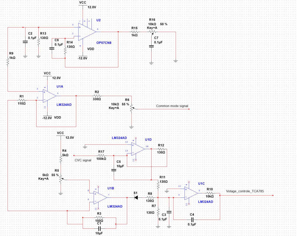
current_voltage_controller.PNG
 
Lets say 0-10 VDC signal in increments of 1 volt or a 0-20 mA signal in increments of 1 mA has given to inverting input of U1D,pin 13, CVC signal.
Why can't you eliminate all that circuitry and just apply that signal directly to the control input of the TCA785?
 
Why can't you eliminate all that circuitry and just apply that signal directly to the control input of the TCA785?

Thank you to take part here.
If you deeply look at the design, you would understand I need signal conditioning before appling to phase control IC.
Mention here what we are going to do, why the OPAs are usually do, what portion of signal we are interested in!
 
If you deeply look at the design,
Well I have looked at your circuit, and most of it does not make sense, most of it does nothing.

U2 does nothing, there is no input signal, the output just connects to ground.

U1a has no input signals, and its output signal is described as an input from some other circuit.

U1b has only one input signal.

What is this thing supposed to do?

JimB
 
Most resistors have values much too low for these opamps to drive.
 
Well I have looked at your circuit, and most of it does not make sense, most of it does nothing.
Kindly find a partial possible solution.

U2 does nothing, there is no input signal, the output just connects to ground.

For some time being, lets assume U2 output is connected to U1A's pin number 3 (not connected to ground) and disconnect the previous connection from pin 3 coming from pin 3 of U2. Lets say pin 3 of U2 is connected to a power source. Connect the pin 2 to ground. Note that, feedback path of U2 has RC component.


U1a has no input signals, and its output signal is described as an input from some other circuit.
If its output is not connect to ground, C-M mode does nothing?

U1b has only one input signal.
It has been taken in a common mode signal.

What is this thing supposed to do?
Need symmetrical phase angle trigger for all phases.
Can you understand anything from this document,**broken link removed**
 
Sorry, your diagram still makes no sense.

The TCA785 uses a DC control signal. High level (near supply) is low power out (late firing), low level (near 0V) is high power out (early firing).

Pretty much the only "conditioning" needed is inverting the analog input if you need a low input to be low power out and making sure the maximum control voltage to the 785 is about 2V less than it's supply voltage.

If you have more than one 785 (eg. on three phase), they all get the same DC setpoint and each IC internally does it's own synchronisation to the phase it's working with.
You would need some isolation circuits etc. but no phase or timing stuff. outside the 785's
 
Sorry, your diagram still makes no sense.
It will be hopefully.

The TCA785 uses a DC control signal. High level (near supply) is low power out (late firing), low level (near 0V) is high power out (early firing).
Kindly post a signal/waveform to understand firing and power level.

Pretty much the only "conditioning" needed is inverting the analog input if you need a low input to be low power out and making sure the maximum control voltage to the 785 is about 2V less than it's supply voltage.

I also agree with you here, the purpose of my circuit might use for this occasion. Give me the way to keep the voltage always less than 2 V. I was trying to apply OP-AMP thus it can make the voltage always constant !


If you have more than one 785 (eg. on three phase), they all get the same DC setpoint and each IC internally does it's own synchronisation to the phase it's working with.
Yes, I am using 3 785.

You would need some isolation circuits etc. but no phase or timing stuff. outside the 785's.
Where I need isolation, give me a schematics please.
 
Kindly post a signal/waveform to understand firing and power level.

There is no waveform!

See the 785 example circuit here:
**broken link removed**

That uses a potentiometer for manual power control, using a 0 - 10V range feeding in to pin 11.
The preset pot on the pin 9 circuit allow the device ramp timing to be set to suit the 10V "just off" point.

It's a bit lower maximum that 2V less than supply (around 10V in that examplem so 5V less).
having the control signal reach 2V less is an working range limit not a requirement.

All you need for 0-10V input (& power increasing with voltage) is a linear inversion so 0V in is 10V out and vice versa.


Isolation is needed as you presumably do not want the whole circuit live and for most practical uses you don't want to switch the neutral to the load, as in the example circuits.

You could trigger an opto-triac from the 785 and use that in turn to trigger the triac gate. eg. MOC3020.
https://www.farnell.com/datasheets/2298461.pdf
 
]
Well I have looked at your circuit, and most of it does not make sense, most of it does nothing.

U2 does nothing, there is no input signal, the output just connects to ground.

U1a has no input signals, and its output signal is described as an input from some other circuit.

U1b has only one input signal.

What is this thing supposed to do?

JimB

Hello Sir JimB,

I have forgot to add a Shunt (comes from rectifiers DC output)that should be add between U2 and U1A inputs, like common mode. Hence, C6/R14 filter could work. Sensing shunt is main fact here.
U2 out put has connected to U1A pin 2.
rc_v.PNG
]
 
The circuit still cannot do anything practical.

Even disregarding impractical resistor values, just the U1C stage is impossible. It's acting as a comparator and the output will not do much other than switch between near positive supply and near negative supply.

You say 50mV signal.

R5 sets a threshold of around 3V on the positive input of U1B.
For the 50mV signal to reach that threshold it needs significant gain. U2 is very low gain and U1A is a unity-gain buffer. The signal can never be high enough to have any effect at U1B; it's output is going to be permanently high so isolated by the diode.


The very low value (110 - 150 Ohm) resistors in multiple places are far too low for the opamp outputs to give any really useful voltage swing. I'd be surprised if you get more than 1 - 2 volts across any of those, far less than the needed range for proper opamp performance. They are just plain wrong.

Are you trying to reverse engineer some piece of equipment? Possibly something that uses some five or six band coded resistors, so you are reading them at 1/10th actual value?
**broken link removed**

That plus one or two mis-traced connections could explain a lot.
 
The circuit still cannot do anything practical.
Lets study more to make it practical.

Even disregarding impractical resistor values, just the U1C stage is impossible. It's acting as a comparator and the output will not do much other than switch between near positive supply and near negative supply.
Are you confused on the points where R7,R8 and R11 meets together? Their parallel input impedance is not compatible with R10 you think?

Yes, C4 doesn't make sense, but without DC feedback can make sense under circumstances if it's part of an overall feedback loop, e.g. PI controller. But hardly with the given low integrator time constants.

You say 50mV signal.
My co-worker said me it has taken from the output. I think the question raise for lower input/output impedance is for lower input voltage.
What maximum voltage you could imagine from such shunt? I am talking about, **broken link removed**
If its 50mV, then current is 100 amps for 0.5mOhm resistance!

R5 sets a threshold of around 3V on the positive input of U1B.
For the 50mV signal to reach that threshold it needs significant gain. U2 is very low gain and U1A is a unity-gain buffer. The signal can never be high enough to have any effect at U1B; it's output is going to be permanently high so isolated by the diode.
.
I do agree with you here, voltage divider gives nearly 3-4volts. The purpose behind using U1A is to maintain a balance in terms of impedance between U2 and U1B. If you forget about U1A and consider the Common mode signal to pin 6 of U1B, then all responsibility goes to U1B!
Think what U1D is doing here,

* it is a standard inverting Opamp circuit.
* R17 is the input resistor
* R12 and C5 are in parallel ! and both are the feedback
The DC gain is: A = -R12/R17 = -100k/130 = 0.00077. That means a 10V input becomes 0.0077V at the output.
I don't think this is a useful signal range.
Whats your opinion ?

Interesting to see the diode action here. Beside that what CVC is acting here, does it trying to control negative inputs of U1C?
 
The opamps have limited output current capability and when connected to such low value load or feedback resistances, they simply cannot function in any useful way.

The output may as well be shorted.

For guaranteed correct operation of an OP07, the load resistance must not be less that about 1K. For the 324, the minimum is more like 2K.
Other circuit conditions may mean practical minimum load resistances are higher still.

Good design practice is to avoid using anywhere near "limit" values when they can be avoided - and with opamp circuits like this, ratios of resistor values are usually the critical part, rather than absolute values.


The current shunt you link to has no isolation and whatever voltage is on the load circuit would be fed directly in to the opamps. Again, that is a totally impossible configuration and not at all compatible with your schematic.


You have not answered the question re. it being an attempt at reverse engineering or recreating an existing piece of equipment?
 

Thank you Sir,

Nice explanation again! This design is a prototype, need to modify it well.
Here we go...

For guaranteed correct operation of an OP07, the load resistance must not be less that about 1K. For the 324, the minimum is more like 2K.
Other circuit conditions may mean practical minimum load resistances are higher still
The load resistance that you are talking about is precisely defined here. At U2 Lets R16 is 0% at the beginning. R15 is always 1 K!
Yes, for U1C you can say its bit higher, let me remove that part!

The current shunt you link to has no isolation and whatever voltage is on the load circuit would be fed directly in to the OPAMP. Again, that is a totally impossible configuration and not at all compatible with your schematic.

This Shunt voltage is supposed to coming from another circuit, my co -worker said its 1.2 v.
From partial sensing like the circuit
en.imgsc1264.jpg

But, I am confused how the signal has been produced, may be from external MCU converted voltage !

I have modified the circuit again.
U2 is rarely used.
J3 and J4 jumpers are open most of the time.

If you consider Shunt voltage at J1, then U2 works like an inverting amplifier !
Now, CVC and PCA signal plays the role.
rc_v_1.PNG


From the datasheet, do you want me to calculate the impedance of capacitor for operating frequency that relates the gain?
If so, could give 1.3volt nearly.


You still have several low-value resistors, making operation impossible.
(eg. R1, 3, 8, 11, 12).

Until operation at DC / steady state conditions is possible, capacitor values are irrelevant.

The connections around U2 are starting to look like a conventional "differential input" circuit, but not quite..
https://sub.allaboutcircuits.com/images/03044.png

Suggest me the required gain for each opamp, I will fix the resistor values.
Yeap also suggest capacitor values, I have randomly use 10u(polar) and 0.1u capacitors.

Your suggested circuit looks like holand current source.
Let me think about it more.
I thing current sensing is also a fact here.
 
Without seeing the entire circuit including all connected parts and input voltage ranges etc., it's impossible to know what gain is needed at any point.
 
Without seeing the entire circuit including all connected parts and input voltage ranges etc., it's impossible to know what gain is needed at any point.

Dear Sir,

Do you think, working of U2 is meaningful ?
Shunt output is connected to its non inverting input. While inverting input is grounded !
Load is connected parallel with feedback component !
Is it a voltage and current feedback amplifier ?

How about this design

shunt_sense .jpg
 
Status
Not open for further replies.

New Articles From Microcontroller Tips

Back
Top