Continue to Site

Welcome to our site!

Electro Tech is an online community (with over 170,000 members) who enjoy talking about and building electronic circuits, projects and gadgets. To participate you need to register. Registration is free. Click here to register now.

  • Welcome to our site! Electro Tech is an online community (with over 170,000 members) who enjoy talking about and building electronic circuits, projects and gadgets. To participate you need to register. Registration is free. Click here to register now.

Transistor questions

Status
Not open for further replies.
apakhira said:
See? Thats what i was trying 2 speculate somewhere in the thread--u cant hav current w/o PD. But instead of using that super-big formula, can i just do something like this?:

No need for that formula in practice, a transistor base is current driven, drops roughly 0.7V, and that's all you really need to know?.

1. Take the value of Ib as required

Yes!.

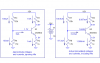
2. Make a potential divider such that v=Vcc/2 (coz its convenient)

Generally it's NOT, you usually want the collector of the transistor fairly close to half Vcc, to allow the maximum voltage swing.

3. Connect the potential divider 2 base with a series resistance Rs such that (Ib*Rs + 0.7)=Vcc/2. Its better if R2 of potential divider be very less, compared 2 Rs, so that potentialdivision does not change much due 2 the load (going 2 base).

It's normal to connect the base directly to the potential divider, to prevent the base current loading the potential divider it should be passing at least five times Ib.
 
It's normal to connect the base directly to the potential divider, to prevent the base current loading the potential divider it should be passing at least five times Ib.
Fine. How do i calculate the required potential 2 b made by the divider, when not using the base resistor and not taking any arbitrary value of the divider (Vcc/2 in my example).Also, if i wanted 2 put Rs there, how many times should Rs be more than R1 and R2 of the divider so that current thru divider is five times Ib (this is just 4 knowledge's sake)?
 
apakhira said:
Fine. How do i calculate the required potential 2 b made by the divider, when not using the base resistor and not taking any arbitrary value of the divider (Vcc/2 in my example).Also, if i wanted 2 put Rs there, how many times should Rs be more than R1 and R2 of the divider so that current thru divider is five times Ib (this is just 4 knowledge's sake)?

As with most things, you apply ohms law and work them out, the voltage drop across Rs makes feeding it from a potential divider pointless, and it would normally be fed from Vcc and be a higher value.

First you need to find Ib - you can do this by dividing the collector current by the gain of the transistor at that current - but transistor gains vary greatly, which is why Rs isn't a good idea, and a potential divider is!.

For a 'standard' transistor example, potential divider for the base, emitter resistor, and collector resistor - everything can be calculated (with as much accuracy as needed) from ohms law, and the single premise that the emitter will be 0.7V lower than the base (for an NPN transistor). You can ignore base current in the emitter, assume emitter current and collector current are identical. Notice at no time did I mention the current gain of the transistor, unless it's a really crappy device it will be high enough to ignore.
 
I think i'm a little lost here. How come when using the voltage divider biasing technique, beta (transisor gain) doesn't affect evrything much? I thought Ic is always related 2 Ib thru hfe. I think u shud explain a bit. I tried searching the net(which is why i'm replying late), but that didnt help.
Also, u cud suggest a few topics which u think i know less about but r essential 4 understanding BJTs.

Thanx
P.S.: R my questions throughout the thread sounding too stupid? If so, pls tell.
 
apakhira said:
I think i'm a little lost here. How come when using the voltage divider biasing technique, beta (transisor gain) doesn't affect evrything much? I thought Ic is always related 2 Ib thru hfe. I think u shud explain a bit. I tried searching the net(which is why i'm replying late), but that didnt help.
Also, u cud suggest a few topics which u think i know less about but r essential 4 understanding BJTs.

Thanx
P.S.: R my questions throughout the thread sounding too stupid? If so, pls tell.

With the standard configuration, of a potential divider on the base, an emitter resistor and collector resistor, and keeping the gain to sensible levels! - you can ignore hfe as it makes less difference than the tolerances on the resistors. The gain of the stage becomes the collector resistor divided by the emitter resistor (negative feedback).
 
Perhaps an actual example would help show you how insignificant Hfe is for a stably biased transistor.
 

Attachments

  • transistor bias.PNG
    transistor bias.PNG
    14 KB · Views: 140
Referring 2 Ron's example, the potential divider is set 2 be at 8.3V. Why has it been set that way? If Vbb is at 1.7V, why taking that potential? And would it matter if we were 2 change R3 and R4 to say 41.5K and 8.5K (keeping ratio same)?
 
apakhira said:
Referring 2 Ron's example, the potential divider is set 2 be at 8.3V. Why has it been set that way? If Vbb is at 1.7V, why taking that potential? And would it matter if we were 2 change R3 and R4 to say 41.5K and 8.5K (keeping ratio same)?

The base voltage is set to give the correct collector and emitter voltages, usually to allow for maximum swing on the collector.

Reducing the values of R3 and R4 won't affect the circuit much, only decreasing the input impedance, and increasing the current consumption.

The potential divider should have a MINIMUM of 5 times the base current flowing through it, increasing that to 10 times is slightly better - with the disadvantages mentioned above.

BTW Ron, thanks for the diagrams and calculations, a fine example of what I was saying.
 
The base voltage is set to give the correct collector and emitter voltages, usually to allow for maximum swing on the collector.
I guess u didn't understand my question:
I know abt the load line, operating point, etc.
I just wanna know how 2 arrive at the voltage, resistor,etc. values when i know Vce and Ic in the required operating point (the whole steps 2 calculate it wud be very good indeed and that'll make it super-clear :) )
 
Last edited:
Hey, please help.How i see it is this:
PD across emitter and gnd is 1V. Considering voltage drop across b-e junction, the potential at base is 1.7V. So shouldn't the potential divider be set to divide the potential at 1.7V? I observe its been set such that Vbb+(PD across base and potential divider node)=Vcc
ie 1.7+8.3=10
Why is it so?
 
apakhira said:
Hey, please help.How i see it is this:
PD across emitter and gnd is 1V. Considering voltage drop across b-e junction, the potential at base is 1.7V. So shouldn't the potential divider be set to divide the potential at 1.7V? I observe its been set such that Vbb+(PD across base and potential divider node)=Vcc
ie 1.7+8.3=10
Why is it so?
Apakhira, you're scaring me. The base divider is set at 1.7V:

10V*17k/(83k+17k)=1.7V.

The emitter voltage is 1V because it is 0.7V below the base voltage.

Maybe I just don't understand what you mean.
 
OK. I'm extremely sorry 4 asking this stupid question. I had made a blunder by calculating Vbb = 10V*83k/(17K+83k)=8.3V
God! I'm scaring myself! How I could i have thought that, when R4<R3? I wonder
why i 4get the basics sometimes while thinking on these things.

OK. Now a better question: what do u do when u want 2 make a class b amp but the input signals peak voltage is less than the "turn-on" voltage of the transistor?
Also, is there any way to make a class B amp where the output levels almost touch the saturation range even though the input levels may be low ( ie can we defy the beta of the transistor)
 
Status
Not open for further replies.

Latest threads

Back
Top