I'm studing transistor right now, but I came out with some practical questions. Some of you may know the JDM pic programmer.
**broken link removed**
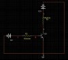
My question are about Q2. Base is conected to 0V across R1, and colector is attached to a RS-232 signal (DTR, aprox +/- 12V) across R2. Chip is fed at 0V and grounded at -5V.
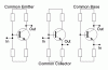
The theory says : when DTR is high (+12V), the transistor works as an emitter follower, with emitter voltage at Vb- 0,7... First problem here. Why? What is really connected to the emitter?? I drawed a diagram cricuit attached. If it is fine, Ve should be 0V, and Vb shoud be 0,7 (common emitter, base biased), and it is not an emiter follower... What is wrong in my diagram??
Many thanks
(also thanks to Nigel, who's been helping me with this so far)
**broken link removed**
My question are about Q2. Base is conected to 0V across R1, and colector is attached to a RS-232 signal (DTR, aprox +/- 12V) across R2. Chip is fed at 0V and grounded at -5V.
The theory says : when DTR is high (+12V), the transistor works as an emitter follower, with emitter voltage at Vb- 0,7... First problem here. Why? What is really connected to the emitter?? I drawed a diagram cricuit attached. If it is fine, Ve should be 0V, and Vb shoud be 0,7 (common emitter, base biased), and it is not an emiter follower... What is wrong in my diagram??
Many thanks
(also thanks to Nigel, who's been helping me with this so far)
")
")
 hi,
hi,