Continue to Site

Welcome to our site!

Electro Tech is an online community (with over 170,000 members) who enjoy talking about and building electronic circuits, projects and gadgets. To participate you need to register. Registration is free. Click here to register now.

  • Welcome to our site! Electro Tech is an online community (with over 170,000 members) who enjoy talking about and building electronic circuits, projects and gadgets. To participate you need to register. Registration is free. Click here to register now.

THEONE's circuit

Status
Not open for further replies.

fabbie

New Member
OK, i think THEONE this posted this diagrams a previous thread to help me out. However, i still dont really understand on how it works. REALLY SORRY ABOUT THAT(might be due to my lack of understanding on certain components). Anyhow, I dont intend to use this circuit, but its good to gain my knowledge on electronics principles.

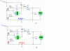
TheONE stated this previously "Look at the 2 diagrams, the input Hi and Lo levels are generated by the switches in the diagram (I had to increase the cap values as I can't change over the switches that fast in the simulation to prevent some discharge of the caps) The PIC will of course do that at 10KHz .
OK, assume the input side of C1 is low (STEP1). C1 will now charge to (5v-1d) and C2 to (5v-2d) where d is the voltage drop over the diode. Now when the input of C1 is forced up to the +5v on the rising edge of the input (STEP 2), this now effectively places the -ve side of C1 on top of the 5v supply. Because the +ve side is now above the 5v line, D1 will now be reverse biased and a voltage of (C1v + 5v) will now be transferred to C2 through D2. The voltage will make the level on C2 to rise up to about 2 times the supply voltage. In this process C1 will discharge, ready for the cycle to repeat again. "

Can anyone please explain(especially THEONE), what are these switches? are they somekind of virtual switch or real switches? i can't see how they automatically on and off themselves.

THX VERY MUCH :D :D (also dont mind telling me what simulation software is this? im need in need of a good one)
 

Attachments

  • 9v_operation_383.gif
    9v_operation_383.gif
    10.2 KB · Views: 425
looks like a voltage doubler cct (or charge pump).

Those switches will be FET's,BJT,relays if you really wanted fet from an oscillator somewhere of approprieate frequency (a few hundred kHz) the true squarewave sent to one switch and an inverted version sent to the other


or use a P-type N-type complementroy pair leg
 
so lets say if im using BJT's as my switch. This would mean i would need 2 supplies, am i right? One to the collector and one to the base( the one to the base would be a high frequency square wave) . Am i right?
 
BJT's as your switches (remember you will need 2) then yep 2 supplies one Power supply and a HF driving square wave

If you use BJT's if you get a NPN and a PNP you can just make a push-pull and use one squarewave to drive both the bases with no inversion needed
 
oohhh.. i get it now.
OK let me get down to the second part i dont understand.

THEONE mention this "Now when the input of C1 is forced up to the +5v on the rising edge of the input (STEP 2), this now effectively places the -Ve side of C1 on top of the 5v supply. Because the +ve side is now above the 5v line, D1 will now be reverse biased and a voltage of (C1v + 5v) will now be transferred to C2 through D2. "

When he said "places the -VE side of C1 on top of 5V", what does he mean by that? i dont see how the capacitor charge can go above the supply.
 
Whan you close SW2 capacitor C1 charges up to abt 4.4V via D1 (5V minus diode drop) and C2 charges to abt 3.8V via D1 and D2 (5V minus 2diode drops)

TheOne sim will have diff voltages since I am running the sim in my head and am using a diode drop of 0.6, TheOne might be using a different diode drop (prolly, 0.4V thus Schokky diodes)


Now with these two charged up (most importantly is the charging of C1, when SWT2 is opened and SWT1 closed you are imposing a zero-loop around C1, the charge on the cap MUST go somewhere to satisfy this condition. Since D1 is blocking this charge going back to the +5V it goes via D2 to C2.

View it as a flow of charge and not of voltages and you will follow what is happening.


Now the switching freq of SWT1 & 2 will be based upon the charging time of C1. If the switching time is too fast then C1 will not charge up to its maximum voltage and thus the output voltage will be lower - you could use this as a way to control the voltage I think???
 
Yes, Styx is correct. The 2 switches can be the internal workings of say a 555 timer, BJT push-pull or anything that switches between the +5v rail and 0v. When the one is on, the other is off. To understand the operation it is important to understand that when SW1 closes the -ve end of C1 is placed at +5v, so the total voltage at the +ve side of C1 will be 5v + C1v (like 2 batteries in series), and this higher voltage (charge) will discharge into C2 through D2
 
ok THX alot. I seem to understand the concept now.
But i dont get 1 last thing. Why do we need C2? It seems to me the most important component here is C1. Since by adding C1 and +5V together, we can obtain almost 2 times the amount supplied by the supply. Is i replace C2 with a resistor, would it be ok? since we are only measuring the voltage drop across C2
 
You need C2 to hold charge (which will supply current to the load) during the replenishing cycle with C1. You can remove it, but then you will have pulsating DC on the output.
 
alright! i get what u mean! thx a bunch

OK since im rather weak with my capacitor theory, dont mind if i ask a basic theory. When the capacitor discharges, current flows out. Therefore, how would i know the amount of current released by it? Do i require a resistor to control the amount of current out of the capacitor?
 
Yes, the amount of current out of C2 will be controlled by the load connected over C2
 
Status
Not open for further replies.

Latest threads

Back
Top