Jeff Birkle
New Member
Switching Regulator Efficiency
Hello,
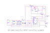
I have made this Switching Regulator and am wondering about its efficiency, and if it can be improved. I calculate it to be 66%. 2 sources have said it should be 74 to 84%.
The input is from 22 to 31VDC
The output is from 4.5 to 6.5VDC at 1.5 to 6A
It on a solderless board for now.
At 1.6A the TIP 31 gets really warm (around 120deg C).
The Components are
IC1 – MC34063
Q1 - Tip31
R1 – 3.3K
R2 – 1.3K
R3 – 15K Pot for Variable output
C1 - 330uF
C2 – 220uF
C3 - 47uF
L1 – 250uH
Any thoughts?
Jeff
Hello,
I have made this Switching Regulator and am wondering about its efficiency, and if it can be improved. I calculate it to be 66%. 2 sources have said it should be 74 to 84%.
The input is from 22 to 31VDC
The output is from 4.5 to 6.5VDC at 1.5 to 6A
It on a solderless board for now.
At 1.6A the TIP 31 gets really warm (around 120deg C).
The Components are
IC1 – MC34063
Q1 - Tip31
R1 – 3.3K
R2 – 1.3K
R3 – 15K Pot for Variable output
C1 - 330uF
C2 – 220uF
C3 - 47uF
L1 – 250uH
Any thoughts?
Jeff
")
