Continue to Site

Welcome to our site!

Electro Tech is an online community (with over 170,000 members) who enjoy talking about and building electronic circuits, projects and gadgets. To participate you need to register. Registration is free. Click here to register now.

  • Welcome to our site! Electro Tech is an online community (with over 170,000 members) who enjoy talking about and building electronic circuits, projects and gadgets. To participate you need to register. Registration is free. Click here to register now.

Supressing voltage spikes using an LC filter

Status
Not open for further replies.

FusionITR

Member
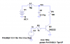
I need to supress voltage spikes at the output of a secondary in a flyback transformer due to a high secondary current flowing into the capacitor's ESR during the transistor off time.

Question is, how do I approach designing an LC filter at the secondary to supress the voltage spikes? Do I just look at this from a straight foward transfer fuction point a view? Such as:

**broken link removed**

Given that H(s) is the amount of attenuation I want at a particular frequency? For example if I wanted to attunuate the voltage spikes by half @ 50Khz (my switching frequency), would I just arbitarily choose an LoCo combination that would yield a 0.5 (absolute) gain at omega = (2)(pi)(50k)?
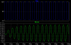
 
You want both the L and C to be large, but the inductor has to carry the load current and it has to fit in the space available, so those are limiting criteria. The capacitor must have low ESR and low impedance at 50kHz and above. Try C = 2200uF and L = 33nH.
 
Where's the feedback required for any switching regulator?
 
The 2200uF caps in parallel (before the LC filter) have esr of 0.018ohms for a parallel equvilient of 0.009 ohm. My peak current in the secondary is 13.77 amp to give a ~0.13V spike I want to attuneate.

Looking at some design articles and my SMPS book, it is stated that the opposite is true of what you said, that both L and C must be small.

Also, actually I was looking more for a mathmatical analysis of the problem instead of just getting component values.
 
Nigel Goodwin said:
Stick some components in and measure the result!.

No thanks... not saying that wouldnt work, its just that I prefer an actual analysis of the system (which is why I bought up the transfer function depiction of the problem). I'm not trying to just "make it work", I'm attempting to learn the design process, using a mathmatical/circuit design analysis.
 
Your input voltage only varies from 16V to 20V - do you really need an isolated DC-DC converter? If not, then a non-isolated synchronous buck regulator would be a better choice. The LC filter would be an intrinsic part of the design. There are many ICs out there that can receive their bias and down convert voltages in that input range.
 
This isn't isolated is it?

It looks like those earths are connected together to me, if not there certainly isn't anything saying so.
 
he stated that this was a simplified diagram - so i am unsure if the two commons are actually tied together or not
 
You need to be careful when you use an LC filter. If your load stimulates it at its resonant frequency, you can get results which are worse than having no inductor. Below is just a simple example, but there are many types of loads that can cause this problem.
 

Attachments

  • LC supply filter waves.PNG
    LC supply filter waves.PNG
    19.8 KB · Views: 374
  • LC supply filter sch.PNG
    LC supply filter sch.PNG
    13.8 KB · Views: 428
You can help minimise this by connecting a parallel LC filter using the same values in series with the load.
 
Hero999 said:
You can help minimise this by connecting a parallel LC filter using the same values in series with the load.
This will add a very high resonant impedance between the load and the supply. Do you really think this is a good idea?
 
Ron H said:
You need to be careful when you use an LC filter. If your load stimulates it at its resonant frequency, you can get results which are worse than having no inductor. Below is just a simple example, but there are many types of loads that can cause this problem.

Yes the two grounds are conneted together so its not DC isolated. I know a buck converter would be more simple design for such a low input voltage and output power, but I have already sucessfuly designed a buck converter (schematic attached at the bottom incase anybody is interested), and want am designing a low power flyback smps for educational value, not praticality (however, after a sucessful test run I will be designing a higher power flyback smps for a pratical use).

RonH - The corner frequency of your LC filter is 151khz but your load transient is only 10khz, why would it oscillate at such a low load transient frequency when the LC filter phase lags 45 degrees all the way out at 151khz (meaning there is basically no lag at 10khz?).
 

Attachments

  • schematic.jpg
    schematic.jpg
    71.8 KB · Views: 341
Last edited:
In order to do a mathmatical analysis, you need to know the characteristics of the load and the source. Both of these are complex, nonlinear quantities, so the best method is computer simulation.
 
FusionITR said:
RonH - The corner frequency of your LC filter is 151khz but your load transient is only 10khz, why would it oscillate at such a low load transient frequency when the LC filter phase lags 45 degrees all the way out at 151khz (meaning there is basically no lag at 10khz?).
Because the load is a square wave, which has harmonics that extend far beyond the fundamental. If one of the harmonics is at the resonant frequency of the filter, it will ring.

EDIT:
You sucked me in there. :) You read something wrong in my sim. The square wave is at the resonant frequency of the filter.
What I said about harmonics is true, but the amplitude of the 15th harmonic will be 1/15th the amplitude of the fundamental.
 
Last edited:
Status
Not open for further replies.

Latest threads

New Articles From Microcontroller Tips

Back
Top