Continue to Site

Welcome to our site!

Electro Tech is an online community (with over 170,000 members) who enjoy talking about and building electronic circuits, projects and gadgets. To participate you need to register. Registration is free. Click here to register now.

  • Welcome to our site! Electro Tech is an online community (with over 170,000 members) who enjoy talking about and building electronic circuits, projects and gadgets. To participate you need to register. Registration is free. Click here to register now.

some trouble making PCBs

Status
Not open for further replies.

bogdanfirst

New Member
ok, i am stuck!
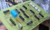
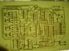
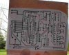
i have designed a 2 layer board, it has tracks both on top and on bottom.
i use the termanl technique to transfer the image from the design to the board.
ok, but now here is the problem.....how do i align the images from the both sides so that the holes will match ?
anybody has got aby suggestions? or maybe some advice from personal experience?
 
Easiest way i have found is to put alignment marks on the layout, then tape a paper printout on the copper and drill the holes out, then go on with the rest and use the holes to line it up. Thats how i did this one:
This is pre-drilled, but notice the small drill holes and marks, i used 3 and it worked out very well. Here are a few pics i took in the process, have a bunch more.
 

Attachments

  • PCB_327.jpg
    PCB_327.jpg
    21.5 KB · Views: 1,029
  • PCB_2.jpg
    PCB_2.jpg
    14.2 KB · Views: 1,121
  • pcb_4.jpg
    pcb_4.jpg
    15.7 KB · Views: 1,022
hmm thats neat! btw what paper are you using? is it an "iorn-on" type?

Another question, how do you create a transparency/negative film for photo etching method. I am using Eagle Cad software and I can only print out the normal tracks, for photo developing I would need an "inverse print" which will allow the film to expose the track areas, any thoughs?

Linux
 
here is a tip for ypu, Linuxking......
check the resolution of your printer, oyu might have 300, 360....something like this, or maybe even more....
anyway, export the pcb as a picture with the resolution of the printer. then go in Paint and modify the colours. then use Imaging to print the picture with the option Pixel to pixel.
and you are done!
ooopp.......you are using windows too? aren't you?

ok, and now for my question to E (?!)
do you make one side and then the other or how?
could you explain the steps you take in making the pcb? please.....
 
bogdanfirst

thanks, it works great! although I had to find a windoze machine for Imaging, I will see if GIMP can do this :)

Linux
 
to make that one, i first designed in a PCB design program, exported it to autocad and mirrored the top side, then i used a command to join all the poly lines, (when it is exported all the lines are broken) then touched up anything neccesary in autocad, it will give you both layers superimposed on each other on differnt layers, works very well for mirroring one side. The design is really the hardest part as far as im concerned.
Then i printed each side onto a piece of that blue iron-on stuff. i also went back and mirrored the whole thing to give me a printout rightside up so i could use it for alignment and such, thats what you see in that one picture it is just normal peper taped on for lining up.
Then i cleaned it real good, and ironed the blue stuff, i tped both sides on and ironed and flipped, worked very well., then i etched. done.
I was really impressed how well that blue stuff worked, that was the first time i ever tried it, it took a few tries to get it right but im impressed at the overall quality.
 

Attachments

  • PCB_stuffed.jpg
    PCB_stuffed.jpg
    16.2 KB · Views: 964
  • after_iron.jpg
    after_iron.jpg
    31.4 KB · Views: 960
ok.....
just one question.......
how do you make the vias? do you put a wire trough the hole and then solder it on both sides or do you have another way?
 
Status
Not open for further replies.

Latest threads

New Articles From Microcontroller Tips

Back
Top