Continue to Site

Welcome to our site!

Electro Tech is an online community (with over 170,000 members) who enjoy talking about and building electronic circuits, projects and gadgets. To participate you need to register. Registration is free. Click here to register now.

  • Welcome to our site! Electro Tech is an online community (with over 170,000 members) who enjoy talking about and building electronic circuits, projects and gadgets. To participate you need to register. Registration is free. Click here to register now.

Some macro photos of see-through electronic components

Status
Not open for further replies.

Fluffyboii

Active Member
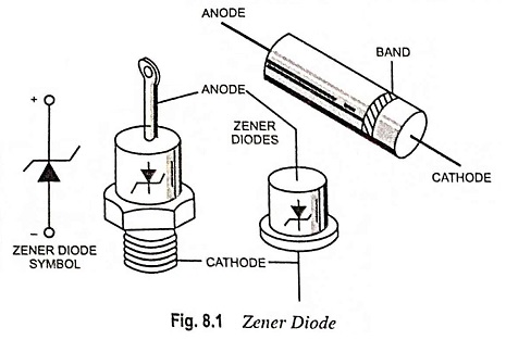
Instead of boring you guys with my non-functional circuit problems I decided to post some macro shots I just took with my new macro lens + close up filter. First two is AAZ15 gold sealed Germanium diode then 4148 Silicon diode, LED, LDR, 6.2V Zener diode. I wanted to see a difference between Zener and Silicon diode but I can't, I guess it is in a microscopic level. Can someone explain the inner structure of these.
 

Attachments

  • DSCF2312.jpg
    736 KB · Views: 297
  • DSCF2313.jpg
    783.8 KB · Views: 294
  • DSCF2314.jpg
    606.6 KB · Views: 304
  • DSCF2315.jpg
    818.3 KB · Views: 288
  • DSCF2316.jpg
    863.4 KB · Views: 274
  • DSCF2317.jpg
    740.8 KB · Views: 287
Very nice!

A zener in principle is a diode that has a deliberately low reverse breakdown voltage, plus being designed to try in minimise the internal resistance so the voltage does not change too much with changes in current.

Many P-N junctions show a similar effect, such as the base-emitter junction of normal transistors, if reverse biased.

I'd guess that even some rectifier diodes may behave rather like high voltage zeners, though the current would have to be extremely small to avoid them being damaged by overheating.
 
Zeners generally have higher doping to reduce the depletion layer than regular diodes to achieve the
higher breakdown voltages.


1663013379147.png


Regards, Dana.
 
Zeners generally have higher doping to reduce the depletion layer than regular diodes to achieve the
higher breakdown voltages.


View attachment 138571


Regards, Dana.
That makes sense, just as they teach in college. Is the shiny, mercury looking thing at the middle of the diode is the silicon. What is the orange/brown section that holds it.
 
If I am not mistaken the die (grey) is sandwiched between two Cu slugs,
to minimize L, R, maximize heat transfer.

The Ge are interestingly enough point contact diodes.


Regards, Dana.
 
If you had your camera on the CRT display of a Scanning Electron Microscope (SEM) then you might see the surface structure. Even LED's have an excellent Zener quality and a much lower series resistance. The 5mm epoxy types are about 10 Ohms for Red/Yellow at 2V 10 mA and 15 Ohms for White at 3V @ 10 mA with some tolerance depending on design/ process. They use transparent substrates so the reflector cup is the cathode and anode has the thin gold wire bond. So the -ve lead is the heat sink.
 
Status
Not open for further replies.

Latest threads

New Articles From Microcontroller Tips

Back
Top