Continue to Site

Welcome to our site!

Electro Tech is an online community (with over 170,000 members) who enjoy talking about and building electronic circuits, projects and gadgets. To participate you need to register. Registration is free. Click here to register now.

  • Welcome to our site! Electro Tech is an online community (with over 170,000 members) who enjoy talking about and building electronic circuits, projects and gadgets. To participate you need to register. Registration is free. Click here to register now.

[solved via schmitt trigger] matrix keypad not recognized at all by 8051 micro

Status
Not open for further replies.

mik3ca

Member
I have a problem with my keypad setup.

I made the following circuit so that the microcontroller can sniff out a unique value based on what key is pressed.

I ordered the keypad from futurlec and the datasheet for it is here: https://futurlec.com/Keypad3x4.shtml

I have tested the keypad by itself and verified it works. I also tested the PCB I assembled my circuit on and there are no short circuits and no cracks in the traces.

I made this circuit instead of using fancy chips because I wanted to use parts that are commonly available in Canada. Here I used the 74HC138 to select a column then the 74HC151 to help decode the signal. Then I tied the inputs of both chips to a 74HC393 binary counter so that every number can get scanned. The microcontroller itself uses a 22Mhz clock (not shown here). I also tied a 10K resistor to 74HC151 output so that I don't blow anything up if I accidentally set the wrong pin to logic low while the chip outputs a high.

This is the best I came up with so far given that I actually only have three I/O pins on the microcontroller left to use along with the reset signal.

Is there any way I can improve this circuit or even do a better circuit that can help a microcontroller determine what button is pressed on a matrix keypad?

I also added my source code for the 8051 microcontroller.
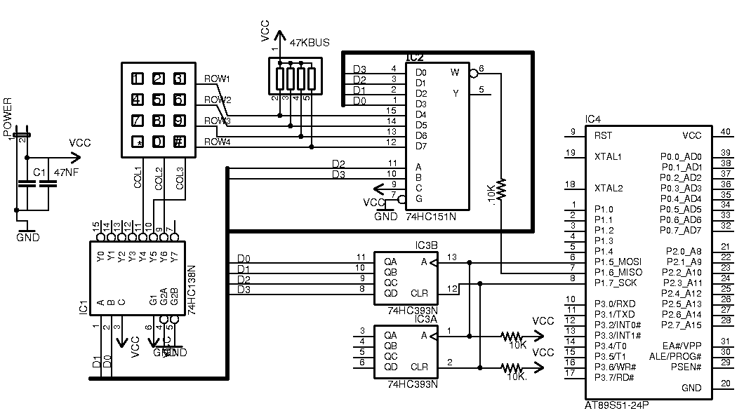
circuit.png


Code:
;individual keys on the keypad:

    _K1 equ 0h
    _K2 equ 1h
    _K3 equ 2h
    _K4 equ 4h
    _K5 equ 5h
    _K6 equ 6h
    _K7 equ 8h
    _K8 equ 9h
    _K9 equ 0Ah
    _Kstar equ 0Ch ;star
    _K0 equ 0Dh
    _Knum equ 0Eh ;pound

    ;other defines

    KPADINC equ P1.5 ;keypad increment
    KPADVAL equ P1.6 ;keypad get val. 1=set
    KPADRES equ P1.7 ;reset keypad. 1=reset
    KPADNUM equ 64h  ;Possible number we want
    KPAD bit 0h      ;Bit indicating button was pressed

    ;Key press
    kpress:
      ;See if a button is down
      jnb KPADVAL,nmatrix
        ;button is down.
        ;see if it was pressed before
        jb KPAD,mxnokeyyet
              ;it wasn't pressed before
              ;wait till button is released
            jb KPADVAL,$
              ;Button released so get value
            mov A,KPADNUM
            anl A,#0Fh
              ;And set flag and exit
            setb KPAD
            ret
        mxnokeyyet:
      nmatrix:
      ;button isn't pressed
      ;so pulse the clock and increment number hardware is at
      setb KPADINC
      inc KPADNUM
      clr KPADINC
      ;and exit
    ret

    mkeys:
      acall kpress   ;Try to get key
      jnb KPAD,mkeys ;and keep trying till we get one
      lcall ktoval   ;then convert value to actual key we pressed
      clr KPAD       ;clear flag so new value can be received
    ret

    ;keypad to raw value A=keypad value. Output: 0Ah=* 0Bh=#, 0-9=num
    ktoval:
      anl A,#0Fh ;input must be from 0-15
      jnz knoz
        inc A ;0 converts to 1
        ret
      knoz:
      movc A,@A+PC ;input wasn't 0, so use table to get value
      ret
    db 02h,03h,0FFh,04h,05h,06h,0FFh,07h,08h,09h,0FFh,0Ah,00h,0Bh,0FFh,0FFh,0FFh
 
The circuit seems to be okay ( there is no need to connect D0 ~ D3 to the 74hc151 for multiplexing as the read is on the top half of the byte ) The circuit would be great for 4 x 4 keypads... The only thing I can see is you are not setting P1.6 to input before you read! Also! if you just read all 16 clock in one you will have a multiple key read...
 
( there is no need to connect D0 ~ D3 to the 74hc151 for multiplexing as the read is on the top half of the byte )
I understand that but seeing that I do PCB's myself and that I'm only limited to single-sided, I might as well include these "hacks" in my circuit so that routing would be substantially easier.

The only thing I can see is you are not setting P1.6 to input before you read!
I think this is an automatic thing with an AT89S52 where the port pin values are always set to logic high once the program begins.

Also! if you just read all 16 clock in one you will have a multiple key read...
My program intends to call the key read function endlessly until any ONE key is detected.
 
My program intends to call the key read function endlessly until any ONE key is detected.
I know... And that end it works! But!! imagine security key entry with four keys pressed simultaneously!! cool or what!

Why do you think it isn't working?? Aha!! Flipped all the JB and JNB .. AND!!! Set P1.7 to low...
Code:
 kpress:
      ;See if a button is down
      jb KPADVAL,nmatrix
        ;button is down.
        ;see if it was pressed before
        jb KPAD,mxnokeyyet
              ;it wasn't pressed before
              ;wait till button is released
            jnb KPADVAL,$
              ;Button released so get value
            mov A,KPADNUM
            anl A,#0Fh
              ;And set flag and exit
            setb KPAD
            ret
        mxnokeyyet:
      nmatrix:
      ;button isn't pressed
      ;so pulse the clock and increment number hardware is at
      setb KPADINC
      inc KPADNUM
      clr KPADINC
      ;and exit
    ret
 
imagine security key entry with four keys pressed simultaneously
Good imagination, but at this time, the keypad will only be used by hardware debuggers of the project such as myself and the user Interface I'll make for the project will be easy enough in which only one key will be pressed at a time.

Aha!! Flipped all the JB and JNB...

jb KPADVAL,nmatrix
Wait a second... I'm trying to understand why your theory works.

The reason why I posted my code as such at the beginning is because when a column on the keypad is selected, a logic low will run through it and the remaining columns will have a logic high through it. If a key on the active column is pressed then the row will also become active low while the other rows will remain high. If the desired row is scanned as well, then this active low passes through the 74HC151 and gets inverted at the output which then produces a logic high output for a pressed key. So I don't understand why flipping the JB and JNB will work.
 
logically a button press is low as you have pullups...

jump not bit tells the chip a button was pressed so the "pressesd button loop" isn't activated.
IF!!! you use "jump bit" that means no button was pressed so carry on with the inc keypad.

I have tested it and it works very well.... I changed the code to read in 16 clocks and now I can have multiple keys... So thanks for that!!
 
hmm.. Maybe eagle is lying again! It already lied about the 74HC393 IC by not showing that the clock is incremented on logic low. So based on the way you're answering the question, either the output resistor would need adjusting or Eagle would be lying about the 74HC151 as well. In any event, I decided to change over to a simpler microcontroller setup.
 
Once again I did another remake. This time I did the original circuit except now I added a schmitt trigger circuit before each 74HC151 input and now I made use of the second counter so I can capture the output much easier.
 
I thought I should post the circuit for reference in case I get stuck. Given what I had on hand, I used 2.2K for all resistors and 47nF for all capacitors. All logic IC's are 74HC series. The jumper switch under the 74HC151 on the right is used to select whether live output should be used or stored output should be used. By stored, the output toggles on each correct key press but since I can reset the whole thing, the stored output also resets. Only drawback with this design (which I will have to deal with) is that I'll have to wait at least 80 clock cycles (1 cycle for 8051's set bit, and 1 cycle for clear bit and 2 for comparison of data and 1 for increment) for the character at row 3, column 4 (the pound) to be scannable each time I reset the circuit after detecting a valid key press. I don't think I can go better than that without using extra IC's.

Now I'm curious, just how low can I go with capacitors without the buttons in bouncy mode? because I tested the 74HC14 on a bread board using the same setup and I find that if I use like a 10pF to 100pF capacitor with 10K resistors then the debouncing wouldn't work but if I used like a 1uF cap then debouncing will work. I expect to press the button at least 6 times a second at most.

circuit.png
 
Ok now i figured it out.

Checking propagation delays of various chips and adding them led me to think it takes 600nS for the chips to process the data. My micro runs at 22Mhz and for a standard 8051 that translates to processing 1 instruction every 22118400/12 or 0.53uS.

I had to add delays (about 256uS) in my code right after I set the clock value and right after setting or releasing reset in order to compensate both for the button release time (from R and C of the schmitt trigger input which I have yet to get a definite equation for) and for the propagation delay. At least now it works
 
Status
Not open for further replies.

Latest threads

New Articles From Microcontroller Tips

Back
Top