Continue to Site

Welcome to our site!

Electro Tech is an online community (with over 170,000 members) who enjoy talking about and building electronic circuits, projects and gadgets. To participate you need to register. Registration is free. Click here to register now.

  • Welcome to our site! Electro Tech is an online community (with over 170,000 members) who enjoy talking about and building electronic circuits, projects and gadgets. To participate you need to register. Registration is free. Click here to register now.

SMD FETs with top heat tabs should never be used?

Status
Not open for further replies.

Flyback

Well-Known Member
Hi,
Do you agree, these SMD FETs with top heat tabs should never be used?....

[EDIT]...This question is in relation to an SMPS PCB inside an aluminium box with a 1cm thickness all round (all 6 sides) .....as such, that will be used for the heatsinking, otherwise its a waste of such a thick box. ie a square box, 4 sides, and top and bottom). The box is approx 20cm x 10cm x 7cm [END OF EDIT]

IAUS260N10S5N019T

Because..
1...They are a rarity and can go nil-stocked easily
2....Its too complicated to do heatsink connection for them (as opposed to bottom tab to thermal vias on PCB, to bottom copper, to insulate pad, to heatsink)
3.....There is no way to search any search engine to find and pull out those SMD FETs with top side heat tab.
4....They are always more expensive to buy.
5.....Their heatsinking arrangement is always more expensive than "normal" SMD FETs...the heatsink needs "gouging out" to make room for the FET....machining from solid.
 
Last edited:
I don't see a problem, if it is an industry-standard package?

Why does anything need machining? The thermal connection is flush with the top of the device, so all it requires is a flat heatsink with a thin conformal pad & the board held / clamped / sprung against it.

When practical & when high dissipation cannot be avoided, I'd much rather have the heat in a separate heatsink rather than the PCB, where it's transferred to other components.

It also leaves the other side of the PCB free for connections or components, rather than that having to be flat and insulated to allow that to be against a heatsink!
 
Why does anything need machining? The thermal connection is flush with the top of the device, so all it requires is a flat heatsink with a thin conformal pad & the board held / clamped / sprung against it.

Thanks, if the device is PCB top mounted, then how do you do that? We need to do it simply, without much requirement for labour intensity.
If the Device is mounted on bottom of board, then because the bottom rests on the flat heatsink, then that heatsink needs gouging out for the protrusion of the bottom mounted SMD FETs....there then needs to be gap pad to interface through the inevitable gap, to the bottom heatsink.

AYK, Simplest way is just to have an all SMD board, mount smd fets on top side, and sit the board on a insulation pad on the flat heatsink (thermal vias through etc etc)
 
Last edited:
Why ask the question when you've made up your mind? Looking for consensus I suppose.

You don't seem to get out much. Here's an example of heatsinks for a Raspberry Pi (an immensely popular single board compter). These are attached to chip using heatsink tape, which serves as a thermal pad and adhesive to hold the heatsink in place. It's about the stickiest and most tenacious tape you've ever seen.

SmartSelect_20221127_090218_Edge.jpg


SmartSelect_20221127_090241_Edge.jpg
 
Thanks,
Yes , i see your point.
My sincere apologies as i should have said...(top post now edited)
In our case, the PCB is inside an aluminium box with a 1cm thickness all round.
As such, it makes sense to use this as a heatsink....
And given that.....top mounted FETs are the best way, would you agree?
 
if the device is PCB top mounted, then how do you do that? We need to do it simply, without much requirement for labout intensity.
Screws through the board into the heatsink to put pressure on the thermal pad.

Going via the PCB to a below-board heatsink will result in a much! higher thermal resistance from the device to the heatsink.

As I said to start with, it's down to the device requirements. if you must use surface mount devices with such high power ratings, you have to provide suitable heatsinking with low thermal resistance.

Personally, I'd probably use a module - I particularly like these series:


Just put clearance holes through the PCB for the device fixing screws, and they bolt direct to the heatsink with just thermal grease, as they have internal insulation.
 
Going via the PCB to a below-board heatsink will result in a much! higher thermal resistance from the device to the heatsink.
Thanks, thats very true......and i am sure you would agree that if an SMD FET does not have a top-side metal heat tab, (ie, its top-side is plastic), then the thermal path to a top mounted heatsink is worse than going through a PCB from a SMD FET with a bottom side heat tab?

Also, SMD FETs with top side heat tabs are very rare, may well go nil-stocked, and are not searchable on digikey or any component site.
 
i am sure you would agree that if an SMD FET does not have a top-side metal heat tab, (ie, its top-side is plastic), then the thermal path to a top mounted heatsink is worse than going through a PCB from a SMD FET with a bottom side heat tab?
Obviously.

I don't see how that relates to the question re. using those top heatsink devices, though?
 
I don't see how that relates to the question re. using those top heatsink devices, though?
Basically, the SMD FETs, with top side heat tab, are so rare (and going obselete), that they are not worth using....it says it all that you cant even search for them. If used, they are most likely to go nil-stocked.

If they are used (top tabbers), then heatsinking is labour intensive if you try and mount heatsink to their top with screws etc...and if you put them under the PCB, then you have to gouge out the aluminium base to make space for them.

I think the thermal resistance of 4 layer PCB, with copper plane on all layers, and multiple thermal vias plated over...going fown to heatsink, is the best way?
 
If they are used (top tabbers), then heatsinking is labour intensive if you try and mount heatsink to their top with screws etc...
You do not "mount" the heatsink - you mount the PCB (to the heatsink).
In other words, you screw it in to the enclosure and the fixing screws provide the required pressure through the PCB and round the devices.

You appear to be wanting things to be complicated. Follow KISS principles!
 
You do not "mount" the heatsink - you mount the PCB (to the heatsink).
...Thanks, yes, thats the way our customer does it in the SMPS they have sent us.....the "top-tab" SMD FETs are mounted to the bottom of the board, and you screw the board to the aluminium baseplate, and put a bit of gap -pad on the fet top, ,and thats it......but you need to gouge out a "pit" in the baseplate, so the fet can protrude into it.
 
the SMD FETs, with top side heat tab, are so rare (and going obselete)
Is that why there are "only" 4,440 hits for that exact package?

Or why Infineon are still introducing new devices using it?

but you need to gouge out a "pit" in the baseplate, so the fet can protrude into it.
No.. Just no. There is no "need" to have anything but a flat mounting surface, to use that device type.

Sorry but a lot of your comments & claims just do not seem to make sense.
 
No.. Just no. There is no "need" to have anything but a flat mounting surface, to use that device type.
Yes i agree, but the PCB is screwed to that same surface....the SMD FET protrudes out from the PCB underside....so you have to gouge out a "pit" for the protrusion of the fet...but yes, the bottom of that "pit" is indeed flat, as you say. I wish i could share the enclosure picture, but unfortunately it would probably be deemed giving away secrets.

I suspect you are thinking to put the "top-tabber" SMD FET on the PCB topside...but then you are not using the thick aluminium baseplate on which the PCB will sit. -ie not using its heatsink properties.....i think you mean to kind of somehow mount a heatsink to that top-tab, with the "Top-tabber" soldered to the PCB topside?
 
Or mount the circuit board with suitable standoffs or washers to put it all the right height.
 
Thanks,
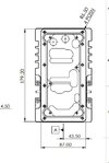
And i presume you would say, having an alu enclosure like the attached made, with the "gouge pits" shown, would be extremely expensive? (The "gouge pits" are so the bottom side FETs and some other components dont snag the base of the enclosure when the PCB is mounted to said same base.)

So the image shows looking down on the enclosure, with the alu top removed, and you can see the base...and the "pits" that have been gouged out.
 

Attachments

  • Alu Enclosure bottom _pits gouged out.jpg
    Alu Enclosure bottom _pits gouged out.jpg
    38.6 KB · Views: 145
I would say it's your job to evaluate machining costs vs. costs for doing it by some other method. It depends on many things, starting with the quantity you're making.

It also means in the board is revised or a different component is used, those enclosures could turn into expensive scrap.

Also, have you taken into consideration exactly what the tolerance is on the fit? If you're using heatsink paste, you ideally want zero clearance between the heatsink and component. If you use a thermal pad, you might get away with more variation.
 
Last edited:
but the PCB is screwed to that same surface.
Sorry, I did not realise you thought I was a mind reader :banghead:

In other words, how on earth does that relate to the fundamental use or not of that specific type of device, with no other restrictions stated, as in the original question!
:banghead::facepalm:
 
Thanks, yes, i do sincerely apologise....-but all of your answers were massively useful anyway.
Now the method is clear......ie, the dreadful "gouged out" enclosure, i am sure all would agree, that those "top tab" FETs are not a good idea here?.........the cost of that gouging must be literally immense?

Ive no idea how much the gouging costs?, unfortunately, i am not privvy to such cost info. I am just told to cut the cost of the components....but.....surely the cost of that gouging outweighs it....and we should use non-top-tab fets instead, and avoid the gouging, and use thermal via heat transfer from "back-tabber" fets?

"Top-tabber" fets look incredibly difficult to heatsink in all circumstances though.,......they lack the convenience of a to220 screw hole for the heatsink.......and need a piece of metal somehow screwed to them , with various bells and whistles, and stuff that'll keep the assemblers too busy. They cant of course, be conveniently thermal via'd to a bottom lying heatsink, like a "back-tabber" fet.

n other words, how on earth does that relate to the fundamental use or not of that specific type of device, with no other restrictions stated, as in the original question!
Thanks, though you have answered the question perfectly in one sense, with your depiction of the complicated assembly routine for these fets above....you depict how more complicated assembly is than a "back-tabber"...thankyou for that.....that was of definite massive interest.
The original question was of interest...its just that also of interest was the specific case of having a thick metal enclosure, (also with a thick bottom) so thick that you are obviously going to use that as a heatsink.
By no means was your answers in any way not useful.

Effectively you did read my mind!...thankyou!..then again my brain is "easy-access" due to lack of grey matter!
 
Last edited:
"Top-tabber" fets look incredibly difficult to heatsink in all circumstances though
with your depiction of the complicated assembly routine for these fets above....you depict how more complicated assembly is than a "back-tabber"

No, what I've been trying to get through to you is that the assembly [as the original question, without the added (and weird) constraint of the entire PCB flat to metal] is that they are trivially simple to heatsink!

PCB_Heatsink.jpg


Heatsink, thermal pad, then the PCB held in place with screws - though if that was a real design I'd add a centre screw to maintain even pressure. No machining, just PCB fixing holes that are needed anyway!

Very simple, and faster assembly than the screwdown modules we use - they need fixing access through the PCB, and nuts need to be positioned in the extrusion grooves to accept them.

PCB_Heatsink_Screwdown.jpg


Having a PCB hard against metalwork for any normal electronics seems crazy to me; the only things I can ever remember seeing like that are some UHF / microwave / SHF radio devices where grounding distances are ultra-critical.

Also, if the enclosure is already a custom machined-from-solid one, the extra milling to add more pockets should be a trivial extra cost.
Cost is generally down to handling and time in the CNC machine, that it takes to remove the bulk metal.
A few small extra pockets in the base would probably change the price by a percent or two, as other than a slight program change and a fractionally longer machining time, there is no change to the overall process.
 
Having a PCB hard against metalwork for any normal electronics seems crazy to me
Thankyou , this is great info!...i will digest your comments.
I am just trying to picture how we can mount the PCB without it being flat to the enclosure (except for the "pocket" bits of course)...
Being flat to the enclosure kind of stops you from causing pcb flexion when you screw it down to the enclosure, i kind of thought?

Sorry but i just cant see how we can have the bottom mounted SMD FETs protruding off the bottom, and then satisfactorily mount the PCB to a totally flat bottom metal base..?.....i mean, yes, we could have standoffs, but theyd need tapped screw holes and you know how bad is tapping aluminium.
 
Status
Not open for further replies.

Latest threads

New Articles From Microcontroller Tips

Back
Top