Continue to Site

Welcome to our site!

Electro Tech is an online community (with over 170,000 members) who enjoy talking about and building electronic circuits, projects and gadgets. To participate you need to register. Registration is free. Click here to register now.

  • Welcome to our site! Electro Tech is an online community (with over 170,000 members) who enjoy talking about and building electronic circuits, projects and gadgets. To participate you need to register. Registration is free. Click here to register now.

Simple High side N-Channel MOSFET driver

Status
Not open for further replies.

clipo

New Member
Hi all,

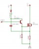
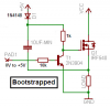
Have just finished a project for work that required a High side low Side N channel MOSFET arrangement so I used a great chip from International Rectifier the IR2106 High Side Low Side Driver and during the project understood how it worked. So whilst I was bored one day I was thinking how I could make my own simple version based on a Boost Strap capacitor the same as the IR2106 and have so far come up with this. It could be useful for some one for a motor driver or some fun project. So far I've had it controlling a PC fan from a PIC 16F628 in a high side configuration and its worked perfect but it might just be a fluke.

So here it is for every one to poke holes in and hopefully I'll learn some thing extra and we will have a little project for the forum and other peoples fun and games...
 

Attachments

  • driver-prototype.jpg
    driver-prototype.jpg
    18 KB · Views: 28,036
The emitter of the transistor drives the gate of your Mosfet. So boostrapping the collector won't do anything. The base voltage of the transistor limits how high the gate voltage will go and if the input signal is up to +5V then the gate of the Mosfet goes up to only +4.3V and it barely turns on.

The transistor should be a common-emitter instead of your emitter-follower. The logic is inverted but the bootstrapping will work when the Mosfet begins to turn on.
 

Attachments

  • Bootstrapped Mosfet.PNG
    Bootstrapped Mosfet.PNG
    27.9 KB · Views: 25,571
A couple of notes about the above circuits:
1) They will not keep the load powered indefinitely because the capacitor will discharge unless the load is switched off & on again periodically. Fine for a PWM circuit; bad for general purpose DC switching.
2) Audio's circuit will only apply 4.3V across the gate/source unless the anode of D1 is connected to a higher voltage such as Vcc.
 
kchriste said:
A couple of notes about the above circuits:
<snip>
2) Audio's circuit will only apply 4.3V across the gate/source unless the anode of D1 is connected to a higher voltage such as Vcc.
I thought that originally, but a simulation says otherwise. With Vcc=20V, and a 10 ohm load, the voltage across the load switched between 0 and 19.8V, although the rise times are terrible due to the 1k pullup.
I don't think Audioguru was necessarily trying to post an efficient circuit - he was just illustrating the bootstrap principle.
 
I thought that originally, but a simulation says otherwise.
I didn't mean that the voltage across the load that would be 4.3V, but between the Gate and the Source terminals of the FET which is OK if it is a logic level FET. This will also contribute to the crappy rise time in a real life circuit. eg as per your SIM: So when the FET is ON then there would be 19.8V on the source and 24.1V at the Gate meaning there is only 4.3V left to turn the FET on.
I don't think Audioguru was necessarily trying to post an efficient circuit
Probably not. More to illustrate the need for a common emitter config as opposed to the emitter follower posted by Clipo.
 
Last edited:
kchriste said:
I didn't mean that the voltage across the load that would be 4.3V, but between the Gate and the Source terminals of the FET which is OK if it is a logic level FET. This will also contribute to the crappy rise time in a real life circuit. eg as per your SIM: So when the FET is ON then there would be 19.8V on the source and 24.1V at the Gate meaning there is only 4.3V left to turn the FET on.

Probably not. More to illustrate the need for a common emitter config as opposed to the emitter follower posted by Clipo.
I didn't read your first post closely enough. :(
 
Audioguru's solution will work but only for AC, the capacitor will eventually discharge though the leakage in the electrolytic and MOSFET's gate.
 
audioguru said:
The emitter of the transistor drives the gate of your Mosfet. So boostrapping the collector won't do anything. The base voltage of the transistor limits how high the gate voltage will go and if the input signal is up to +5V then the gate of the Mosfet goes up to only +4.3V and it barely turns on.

The transistor should be a common-emitter instead of your emitter-follower. The logic is inverted but the bootstrapping will work when the Mosfet begins to turn on.


Thanks for all your replys guys my understanding of this circuit is growing by the second..

Audioguru.. I cant seem to figure out how your boots capacitor would help since it would always be charged up to the +5V supply and not boost the supplt across the FET, I originaly was thinking about the arrangment you sugested but thought the emitter-follower arrangement would work and allow for the logic to be the right way around, how come the boost strap capacitor wont allow the gate voltage to go above the 4.8V since Im going to be driving some large FETs that require a larger threshold voltage and to also speed up the switching times..
Also I noticed you changed the diode on the boost strap how come you chose that one im just going to find the data sheet now.

kchriste.... Im planning on using the design in a PWM system and so the cap charge should be refreshed all the time, Im also thinking of a DC - DC converter and that too would be PWM but as you said it requires longer on times and could cause problems...

Ron H... I'm interested in what software package you used to simulate the design in so I can run my own simulations too, and if you could send me your simulation if the package is free/easily avaliable.

Alternative designs or ideas are welcome Im currently thinking about audioguru's design but adding an extra stage to keep the logic the right way around since Im initialy driving the design from a PIC.

Thanks every one..

Clipo
 
Last edited:
clipo said:
Thanks for all your replys guys my understanding of this circuit is growing by the second..

Audioguru.. I cant seem to figure out how your boots capacitor would help...
I increased the supply voltage of the transistor so the Mosfet has enough gate voltage to fully turn on.
The capacitor charges to 11.3V then it boosts the gate voltage up to +23.2V.

Also I noticed you changed the diode on the boost strap how come you chose that one im just going to find the data sheet now.
You had a very slow rectifier diode that is made for 100Hz. I selected a very fast diode.
 

Attachments

  • Bootstrapped Mosfet.PNG
    Bootstrapped Mosfet.PNG
    35.3 KB · Views: 69,819
audioguru said:
I increased the supply voltage of the transistor so the Mosfet has enough gate voltage to fully turn on.
The capacitor charges to 11.3V then it boosts the gate voltage up to +23.2V.

Many thanks I can see it now, just been deleting and redrawing what happens and its making more sence now, I'll put this circuit together over the weekend on my prototyping board and have a play with it..

Thank you once again.

Clipo
 
Last edited:
many thanks to every body whoo has contibuted so far to this issue...
i am trying to drive by n channel high side but, its is not working... the output of my microcontroller is connected to ir2110 but the HO of the ir2110 is just always on ...please what could be the problem...my switch frequency is 19.52khz.

Hi,
You will have to explain what you are trying to do, and show us your circuit and operating method, by the sounds of it you have got it connected wrong but thats a pure guess.

Also this is a very old thread now but is good you search before posting, so it might take a little for people to remember what they did. i.e. me...
 
none of those is reliable ... eventually the base current discharges the capacitor.

they only work for PWM circuits that have some maximum duty cycle so that the off time can recharge the capacitor
 
I increased the supply voltage of the transistor so the Mosfet has enough gate voltage to fully turn on.
The capacitor charges to 11.3V then it boosts the gate voltage up to +23.2V.


You had a very slow rectifier diode that is made for 100Hz. I selected a very fast diode.

i use this bootstrap circuit (for my knowledge) to drive a dc 12vfan for pc with
800 ohm resistance as a load and the pwm signal is coming from a micro to
the base of the npn transistor the vgate is becoming a pwm signal with a peak of 1v so the fan couldn't be turned on can you please help me how i can fix this problemn??
 
Last edited:
i use this bootstrap circuit (for my knowledge) to drive a dc 12vfan ....
Which circuit? There are a few circuits in this thread.
Attach the schematic and show where you measured only 1V.
Did you use an oscilloscope to measure the 1V pulses?
 
Status
Not open for further replies.

New Articles From Microcontroller Tips

Back
Top