Continue to Site

Welcome to our site!

Electro Tech is an online community (with over 170,000 members) who enjoy talking about and building electronic circuits, projects and gadgets. To participate you need to register. Registration is free. Click here to register now.

  • Welcome to our site! Electro Tech is an online community (with over 170,000 members) who enjoy talking about and building electronic circuits, projects and gadgets. To participate you need to register. Registration is free. Click here to register now.

Routing problems in ORCAD PCB editor

Status
Not open for further replies.

Psytrox

New Member
Hello,

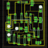
As the title states, im having some problems with ORCAD PCB editor. When I rout the curcuit, everything looks like it has been routed propperly, all the connections made. But in the resaults it says there are two "unconnections", and that it is only 94% complete. Normaly the errors would be marked with red on the curcuit, but in my case it isnt. So I've tried spacing everything out, to see if that helps, but unfortionatly it doesnt.

Has anyone encountered simuler problems, or know what could be wrong?
 

Attachments

  • ScreenHunter_03 Jan. 21 17.23.gif
    ScreenHunter_03 Jan. 21 17.23.gif
    5.2 KB · Views: 382
  • ScreenHunter_02 Jan. 21 17.22.gif
    ScreenHunter_02 Jan. 21 17.22.gif
    29.3 KB · Views: 529
Last edited:
Have you checked the ratnest to see where the 2 problems are? I've had the same problems in the past, but getting into the habit of running the trace all the way to the connect point on the pad eliminated that issue. That might be your problem, but ratnest it and see if editing the disconnected traces shown fixes it.
 
Thanks for the help :) I found the problem. The autorouting wasnt able to place one wire. So it decided not to do anything about it, and I'm guessing it thought I wouldnt notice. One would have thought if a program cost $10 000 there wouldnt be bugs in it :D
 
Well good! But remember to toggle the ratsnest to locate any unconnected nets when either using autoroute or hand routing. I only use autorouting for final component placement, then delete the traces and hand route. I just don't like all the vias and orthogonal trace routing like your board above shows, but that is just my preference.
 
I don't really have that much experience making PCB's, so I find it easier to place componants where I want them, and use the autorouting function. If you don't like the sharp corners, you can use the "gloss" function, which trys to make the 90 degree corners to 45 degree corners.
 
I understand what you believe from your confessed perspective of someone with limited board design experience. My very first attempt at such was back in 1972 or '73 for a US defense agency as a lowly technician, long before any software for such was even envisioned. As you progress with more complex layouts with greater component count and frequency reactance considerations sans proprietary software designed with those considerations, perhaps you will think back to this discussion.

Good luck in your endeavors,
Merv
 
Status
Not open for further replies.

Latest threads

New Articles From Microcontroller Tips

Back
Top