Continue to Site

Welcome to our site!

Electro Tech is an online community (with over 170,000 members) who enjoy talking about and building electronic circuits, projects and gadgets. To participate you need to register. Registration is free. Click here to register now.

  • Welcome to our site! Electro Tech is an online community (with over 170,000 members) who enjoy talking about and building electronic circuits, projects and gadgets. To participate you need to register. Registration is free. Click here to register now.

Question: DC analysis of a transistor amplifier?

Status
Not open for further replies.

samy555

Member
I could not complete the analysis of this circuit.


This is what I managed to do:

IB1 = (VCC - VBE1)/R3 = (3 - 0.7)/100K = 23uA

If β = 100, then IC1 = 2.3mA

VCE1 = VCC – IC1 * R1 = 3 – (2.3m* 2.2K) = - 2.06 V (Error)

The Voltage between points A & B (VAB) = 0.7 volt

So, IC1 = VAB/ R1 = 0.7/2.2K = 0.318 mA

Then, VCE1 = 3-0.7 =2.3 V

I stoppedhere. I wish I couldcalculate IC2 and VCE2 to complete the picture.

Thank you.
 
no circuit attached to post
Edit: After becoming a member at EDAboard forum I now see the circuit.
 
Last edited:
The schematic is at the EDAboard forum.
The horribly biased first transistor is supposed to have an impossible to find and temperature-sensitive hFE of 100 with a base current of 23uA. Then its collector current is 2.3mA. Since its collector load is a 2.2k resistor parallel with the base-emitter of a PNP transistor then the 2.2k resistor has a current of 0.7v/2.2k= 0.32mA then the base current of the PNP transistor is 2.3mA - 0.32mA= 1.98mA. The PNP transistor might also have an hFE of 100 then its collector current is trying to be 198mA. The collector load on the PNP transistor is 64 ohms so its collector is trying to pull up to 198ma x 64 ohms= 12.7V which is impossible with the 5V supply so the PNP transistor is saturated.
 
I don't see it as a bad design.
I rather think it is a fairly good design that needs to be analyzed with experience.

It is just an analysis of a non-inverting High-side switch.

Zin = 100K input impedance
Zload =64Ω load
Vin = Vcc=3V

The load could be a high power relay coil or some other active load.
Each resistor is calculated carefully based on assumptions for the current gain hFE when in linear mode for the 1st stage and when saturated in the second stage as a switch. Unfortunately some interpolation for hFE vs Vce needs to be done from the data sheets, so I'll explain this later.

Let's start with a simple analysis and explain the assumptions.
We know that Vbe starts below 0.6V and rises above 0.7V when Vbe gets saturated due to intrinsic bulk resistance and often well beyond at rated base current.

1. From std. datasheets, hFE= 200 nominal for both Q1 & Q2
2. Let Vbe1= 0.6V since base current is very small (3-0.6V)/100k= 24 μA,, but Vbe will be 0.7V or more, assume 0.7 now.
3. Ic1 = 200*24uA = 4.8mA minus the current thru R1, which was designed to be a bit more than 5% of Ib2 ,

  • I_R1 = Vbe2/2.2k = 0.32mA so Ib2 = 4.5mA
  • almost 95% of collect current ends up driving Q2, which is good for a sensitive fast switch.
4. The main trick here not taught in school, is that when Transistor Vce saturates, they are always rated at only fixed current ratios like Ic/Ib=10 or 20 or 50 .
  • then they give the Vce(sat) result at two current levels for Ic/Ib=x, so you may have to interpolate.
  • If you design for Ic/Ib= spec ratio, then you can get specific range of results for Vce(sat).
  • The trick to remember is that when saturated, the current gain tends to be around 10% of the linear hFE for a reasonable low Vce(sat).
  • So we are going to use a current gain of 10% of 200 or Hfe(sat) = 20 to compute Ic2.
5. We conclude that Q2 is saturated, because Ic2= 20x4.5mA=90ma . if linear across R5 would be 5.76V
  • Since Vce2 is saturated R5 should be near 2.9V thus Ice2=2.9V/64Ω= 45mA
  • we see from the datasheet for a ratio of 10:1 is used to give Vce(sat)
  • here Ic/Ib= 45/4.5mA .. Eureka 10:1 ratio was used.
R1 serves a purpose when the input goes low to speed up the switch off time.

For a quicker analysis we see Q1 will never saturate as the collector is always 1 diode drop below Vcc
We see that will saturate Q2 if the load current/base current is 10:1

So to recap, we calculate
Ib1
hFE*Ib1=Ic1
assume Q2 saturates with no Collector feedback then verify Ic/Ib ratio for Q2
then Ic2~ Vcc/R5
then Ib2= Ic1- 0.7/R1 and Ic2/Ib2 is pretty close to exactly 10.
If 20 was used, some devices might give Vce2=0.2 instead of 0.1 , but note in the datasheet the worst case is given as

@25'C
V CE(sat) Collector-Emitter Saturation Voltage
(Ic =10mAdc, I B =1.0mAdc) 0.25V max dc
(Ic =50mAdc, I B =5.0mAdc) 0.4V max dc

2nd iteration.

Since Ic = 45 is pretty close to 50mA we can expect worst case slightly less than Vce2=0.4 and typical since not given, might be half of max.

So we would say Vc2 on R5 is between 2.6~2.9V or 2.75 +/- 0.15

and remember to look for better transistors with ultra low Vce(sat) from Diodes Inc and Fairchild ( not a plug) often rated by Rce[Ω] at ratios of 50

But close enough for government work......
 
The circuit is not a switch. It is a horrible Hearing Aid Circuit: https://circuitdiagram.net/?s=cheap+hearing+aid

I simulated it and it distorts very badly. The output begins muted then gets louder and louder while the distortion becomes unbearable.
 

Attachments

  • cheap hearing aid circuit.png
    cheap hearing aid circuit.png
    83 KB · Views: 133
Since I noticed this is not used for a switch on EDA but a hearing aid amp.

I posted there as below

This may be better for you, and still cheap.

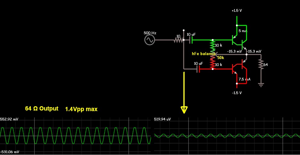
Voltage Gain = 1000= 60dB with 64 Ohm load. Zin =32
Pot added to balance hFE between NPN and PNP,
hfe >300 suggested
Design chosen for max voltage gain but no impedance gain.
Previous stage must be complementary emitter follower. then it can be DC coupled instead of AC coupled.

Batteries are split to load. +/-1.5

1713291100_1439935702.jpg
 
If you really want to re-invent the wheel and find out it squeaks of draws too much current or is too distorted.

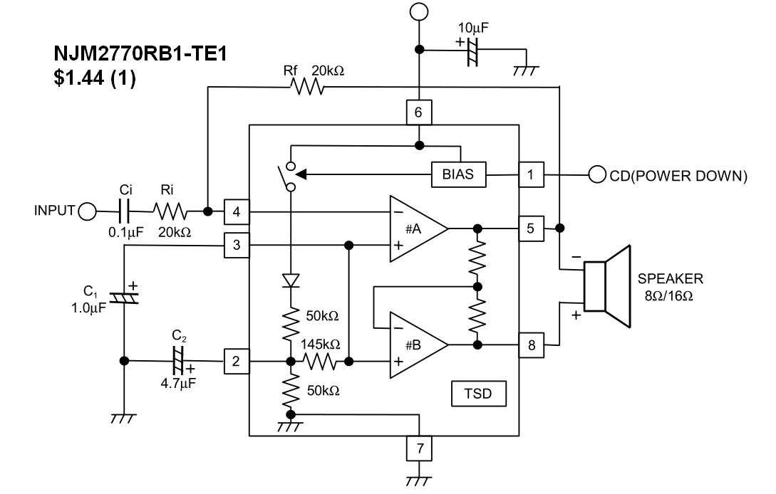
Otherwise, Integrated solutions are far superior. Gain controlled by fixed R values added with Vcc 2~5V ,PSSR = 50 dB, 0.1nA in power down mode, 85dB gain open loop, Vout=0.95 to 1.25Vpp @3V, 0.1% THD @ 100mW

And only $1 in 100pc
9587275500_1439938091.jpg
 
Status
Not open for further replies.

New Articles From Microcontroller Tips

Back
Top