Continue to Site

Welcome to our site!

Electro Tech is an online community (with over 170,000 members) who enjoy talking about and building electronic circuits, projects and gadgets. To participate you need to register. Registration is free. Click here to register now.

  • Welcome to our site! Electro Tech is an online community (with over 170,000 members) who enjoy talking about and building electronic circuits, projects and gadgets. To participate you need to register. Registration is free. Click here to register now.

Programmable Current Source Using LTC3623

Status
Not open for further replies.

vne147

Member
Hello again. I’m having some difficulty with a project I’m working on, and I’m hoping someone can help me find a solution.

I’m attempting to use the LTC3623 as a programmable current source by replicating the circuit shown here:

http://www.linear.com/solutions/7390

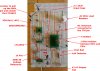
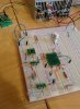
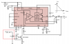
My test circuit is slightly different but I believe equivalent to the schematic shown at the link above. I’ve replaced VSHUNT in the lower left hand portion of the schematic with an ADR130 0.5V precision voltage reference and a 1kΩ potentiometer. I attached another schematic showing the modification I made highlighted in red. Everything else in the schematic is the same.

My problem is that the circuit isn’t working at all. Right now I have it connected to a supply voltage of 6V, and a load of .22 Ω. No measurable current flows for any potentiometer setting and when I measure the output voltage it's around 10 mV. When I remove the .22 Ω load resistor and measure the output voltage, it’s around 100 mV and only changes about ± 10 mV over the full adjustment range of the potentiometer. Obviously this is not what I expected because I used the same op amp, MOSFET, and component values shown in Linear’s schematic.

So naturally I have a few questions:
  • Correct me if I’m wrong, but the MOSFET symbol shown in the schematic is for a P-Channel MOSFET, yet the part number called out (BSC019N02KS) is for an N-Channel Power MOSFET. Can anyone infer enough about what is going on in this circuit to say for sure whether that MOSFET should be N channel or P channel?
  • Also, the MOSFET called out in the schematic is for a pretty beefy SMD MOSFET rated for over 100W. I can’t figure out for the life of me why that would be necessary. Can anyone shed light on that?
  • I have the LTC2054 op amp V+ connected to 3.3V and V- connected to ground. I have also tried it with V+ connected to the same 6V supply as the LTC3623. Both configurations yielded equally unsuccessful results. Does anyone know how I should connect the LTC2054?
  • Can anyone see any problems with my test set up or potential issues that I didn’t address?

Here are links to some datasheets:


Please let me know if I need to clarify anything. Thanks in advance for any help you can provide.
 

Attachments

  • LTC3623.png
    LTC3623.png
    100.8 KB · Views: 157
  • Correct me if I’m wrong, but the MOSFET symbol shown in the schematic is for a P-Channel MOSFET, yet the part number called out (BSC019N02KS) is for an N-Channel Power MOSFET. Can anyone infer enough about what is going on in this circuit to say for sure whether that MOSFET should be N channel or P channel?
Hy VNE,

The MOSFET symbol shown on the data sheet is an alternative symbol for an NMOSFET. The circuit function does require an NMOSFET as you say.:)

spec
 
  • Also, the MOSFET called out in the schematic is for a pretty beefy SMD MOSFET rated for over 100W. I can’t figure out for the life of me why that would be necessary. Can anyone shed light on that?
It does appear to be an extraordinarily hefty NMOSFET for the job required, but it has a very low gate threshold voltage (1.2V), a very low on resistance, and unusually low drain leakage current (1uA) and those are the characteristics that are required, rather than the high maximum drain current. Also, although the NMOSFET has a very high current capability, it only has a maximum VDS of 20V. MOSFET performance has improved radically in the last few years and there are now smaller NMOSFETS that would do the job.

One possibility is that the NMOSFET is oscillating at a high frequency: try putting a 47 Ohm resistor (gate stopper) physically on the gate terminal of the NMOSFET and in series with the opamp output.

Another possibility is that the feedback loop, around the NMOSFET and opamp is oscillating. This may be due to the layout of your circuit and lack of decoupling. A 100nF ceramic capacitor is needed across the supply pins of the opamp.

spec
 
Last edited:
  • Can anyone see any problems with my test set up or potential issues that I didn’t address?
I see nothing wrong, but as previously stated, physical layout and lack of decoupling may be a problem.

The opamp is a low power type with a low open loop frequency response and a limited current drive capability. It is also a self correcting switching type. In addition to the 100nF decoupling capacitor mentioned above make sure that there is a capacitor across the 0.5V reference voltage and a capacitor from the non inverting input of the opamp to 0V.

One test you can do is to measure the voltage between 0V and the non inverting input of the opamp and then measure the voltage on the inverting input of the opam. Both voltages should be identical. Try this test for min and max settings of the potentiometer.

Another possibility is that your PMOSFET gate threshold voltage is higher than specification.

Another test you can do is to replace the NMOSFET with a small signal bipolar junction transistor: BC456, BC547, BC548, BC107, BC108, BC109, BC184, BC183, BC182 would be ideal. Once again, the voltage on the inverting and non-inverting inputs to the opamp should be the same

Can you post a picture of your circuit so that we can see the layout?

spec
 
Last edited:
Spec,

Thanks for the comment and clarifications.

It does appear to be an extraordinarily hefty NMOSFET for the job required, but it has a very low gate threshold voltage (1.2V), a very low on resistance, and unusually low drain leakage current (1uA) and those are the characteristics that are required, rather than the high maximum drain current. Also, although the NMOSFET has a very high current capability, it only has a maximum VDS of 20V. MOSFET performance has improved radically in the last few years and there are now smaller NMOSFETS that would do the job.

Understood. Although, the LTC3623 is a relatively new part I believe. I'm surprised then that the designers didn't use one of the new fangled smaller MOSFETs that are now available. But it makes sense if it was chosen primarily for the characteristics you cited and the fact that it was serious overkill in other areas was just accepted.

One possibility is that the NMOSFET is oscillating at a high frequency: try putting a 47 Ohm resistor (gate stopper) physically on the gate terminal of the NMOSFET and in series with the opamp output.

I tried placing a 47Ω resistor between the output of the op amp and the gate of the MOSFET. No difference from before.

Another possibility is that the feedback loop, around the NMOSFET and opamp is oscillating. This may be due to the layout of your circuit and lack of decoupling. A 100nF ceramic capacitor is needed across the supply pins of the opamp.

Although I didn't mention it and the schematic doesn't reflect it, I do have a 100 nF bypass cap between the V+ and V- pins of the op amp.

I did a little more tinkering and I have some extra data which may or may not help narrow down the problem.

I measured the op amp output for various potentiometer settings. With the V+ pin of the op amp connected 6V and the V- connected to ground, the output of the op amp stays at 6V until wiper voltage of the pot is around 280 mV. As the wiper voltage decreases further, the op amp output also decreases. The op amp output goes down to near zero when the wiper voltage is near zero. I haven't plotted the relationship but it seemed non-linear to me just watching the rate of change on my multimeter.

Does this make sense to you or would you have expected something different?
 
In addition to the 100nF decoupling capacitor mentioned above make sure that there is a capacitor across the 0.5V reference voltage

There is already a 100 nF cap there.

and a capacitor from the non inverting input of the opamp to 0V.

There is no cap there. I'll add one.

One test you can do is to measure the voltage between 0V and the non inverting input of the opamp and then measure the voltage on the inverting input of the opam. Both voltages should be identical. Try this test for min and max settings of the potentiometer.

I'll do the tests you mention here and report back.


Can you post a picture of your circuit so that we can see the layout?
c

I'll also post some pictures. I'm not sure how much they'll help though because some of the jumpers are under components and not visible.

Thanks!
 
Thanks for the comment and clarifications.

No probs VNE. :)

Understood. Although, the LTC3623 is a relatively new part I believe. I'm surprised then that the designers didn't use one of the new fangled smaller MOSFETs that are now available. But it makes sense if it was chosen primarily for the characteristics you cited and the fact that it was serious overkill in other areas was just accepted.
That is the case for many designs.

I tried placing a 47Ω resistor between the output of the op amp and the gate of the MOSFET. No difference from before.
Oh dear! I would keep the 47 Ohm resistor in circuit though. The 47 Ohm resistor will not affect the operation or accuracy of the circuit.

Although I didn't mention it and the schematic doesn't reflect it, I do have a 100 nF bypass cap between the V+ and V- pins of the op amp.
Good move.

I measured the op amp output for various potentiometer settings. With the V+ pin of the op amp connected 6V and the V- connected to ground, the output of the op amp stays at 6V until wiper voltage of the pot is around 280 mV. As the wiper voltage decreases further, the op amp output also decreases. The op amp output goes down to near zero when the wiper voltage is near zero. I haven't plotted the relationship but it seemed non-linear to me just watching the rate of change on my multimeter. Does this make sense to you or would you have expected something different?
No, afraid that is completely wrong.

The voltage on the non-inverting input of the opamp and the voltage on the inverting input of the opamp should always be identical. That is true for all linear circuits using opamps. An opamp's only function in life is to try its best to make both of its inputs the same by adjusting its output.

Just one point, is your multimeter digital and does it have a have a high input resistance of 1M Ohm or higher, or is it an analog multimeter with a needle pointer?

spec
 
Is the 10K potentiometer actually 10K or is it a lot higher in fact?

I meant to ask, what is the voltage on the NMOSFET drain.

Is the 10K resistor connected to the NMOSFET source actually 10K Ohms?

spec
 
No probs VNE. :)
No, afraid that is completely wrong.

The voltage on the non-inverting input of the opamp and the voltage on the inverting input of the opamp should always be identical. That is true for all linear circuits using opamps. An opamp's only function in life is to try its best to make both of its inputs the same by adjusting its output.

To be clear, I was measuring the voltage at the non-inverting input and comparing it to the op amp output, not the inverting input. Does that change what you're saying at all?


No probs VNE. :)
Just one point, is your multimeter digital and does it have a have a high input resistance of 1M Ohm or higher, or is it an analog multimeter with a needle pointer?

It is a low quality Chinese piece of sh*t, but it is a digital multimeter.


Here are some pics. I'm still working on doing the test you recommend and answering the other questions.
 

Attachments

  • Circuit Labeled.jpg
    Circuit Labeled.jpg
    959.1 KB · Views: 172
  • Test_Setup_1.jpg
    Test_Setup_1.jpg
    1.6 MB · Views: 155
I should be back on air in about eight hours- bed here time now.:)

spec
 
Is the 10K potentiometer actually 10K or is it a lot higher in fact?

It's a 1KΩ pot, not a 10kΩ pot. I measured it from end to end and it's 1.009 kΩ.

I meant to ask, what is the voltage on the NMOSFET drain.

The voltage at the NMOSFET drain varies from about 280 mV to 500 mV.
When the voltage at the non-inverting input of the op amp is between ~280 - 500 mV, the NMOSFET drain voltage stays the same at around 280mV
When the voltage at the non-inverting input of the op amp goes below ~280 mV, the voltage at the drain of the NMOSFET starts to rise and tops out at 500 mV when the voltage at the non-inverting input of the op amp is near zero.

Is the 10K resistor connected to the NMOSFET source actually 10K Ohms?
spec

The 10k resistor between the NMOSFET source and ground measures 9.88 kΩ.
 
Is the 10K potentiometer actually 10K or is it a lot higher in fact?

I meant to ask, what is the voltage on the NMOSFET drain.

Is the 10K resistor connected to the NMOSFET source actually 10K Ohms?

spec

Understood. Thanks for your help. I'll do all the other tests in the meantime and post the results here.
 
One test you can do is to measure the voltage between 0V and the non inverting input of the opamp and then measure the voltage on the inverting input of the opam. Both voltages should be identical. Try this test for min and max settings of the potentiometer.

For the minimum potentiometer setting:
inverting = 40mV
non-inverting = 1.5mV

For the maximum potentiometer setting:
inverting = 285 mV
non-inverting = 502 mV

It would appear something is very, very wrong.

EDIT#1:
I had another LTC2504 so I soldered that onto the protoboard and performed the test again. Same results.

EDIT#2:
I also tried completely removing the NMOSFET from the test circuit just to see what would happen. This left the op amp output floating and the inverting input of the op amp connected to ground through a 10 kΩ resistor. The test measurements were:

For the minimum potentiometer setting:
inverting = 39 mV
non-inverting = 2.2 mV

For the maximum potentiometer setting:
inverting = 38 mV
non-inverting = 502 mV

Edit#3:
I swapped the NMOSFET for a BC548 keeping the 47Ω resistor between the op amp output and the base of the BC548. I then performed the same measurements as above and when I did, the voltage at the inverting and non-inverting inputs of the op amp matched exactly for all potentiometer settings. Does that implicate the NMOSFET as the problem?

The circuit as a whole is still not working though. Even with the BC548 in place of the NMOSFET, the output of the LTC3623 never gets above about 1mV or so.
 
Last edited:
Solderless breadboards are notoriously problematic for high frequency switching power circuits.

They have stray resistance, inductance and capacitance that just plays havoc with noise sensitive feedback circuits in switching power supplies..

I suspect that if you looked at the SW node with an oscilloscope you'd see a very narrow pulse at the switching frequency. Narrow, because the pulse gets terminated the instant that it turns on due to the parasitic resistances, inductances and capacitances of the breadboard.
 
Afraid that ChrisP58 is correct in post #14.

If you look at the pictures in the application report you will see that a ground planes and a compact layout are used.

spec
 
Solderless breadboards are notoriously problematic for high frequency switching power circuits.

They have stray resistance, inductance and capacitance that just plays havoc with noise sensitive feedback circuits in switching power supplies..

I suspect that if you looked at the SW node with an oscilloscope you'd see a very narrow pulse at the switching frequency. Narrow, because the pulse gets terminated the instant that it turns on due to the parasitic resistances, inductances and capacitances of the breadboard.

I connected my oscilloscope to the SW node as you mentioned and attached a picture. The time scale was set at .5 μs/div, and the Y scale was set at 5V/div. My oscilloscope is pretty old so that settings aren't exact, and that was the best picture I was able to get, sorry.

Analyzing the waveform though, it seems to be around 1 MHz which is what the datasheet says the frequency should be after connecting the RT pin to the INTVCC pin.

Is the shape and magnitude of the waveform what you were expecting to see? In other words, is it consistent with what you suspect is going on?

I knew that the solderless breadboard would be noisy, and that I would get poor performance in the test circuit. I was just hoping to verify that the circuit was at least functional before committing to it and spending the money to have it fabricated.

Afraid that ChrisP58 is correct in post #14.

If you look at the pictures in the application report you will see that a ground planes and a compact layout are used.

spec

In my PCB design I'm using a ground plane, and the layout is as compact as I could make it. I tried to follow the recommendations in the "Board Layout Considerations" section as closely as possible. This likely futile exercise at bread boarding the circuit was just my attempt to ensure I didn't need to go through several expensive iterations of having the PCB fabricated.


In other news I made a little progress last night. By changing the layout slightly, I was able to get at least a little output from the LTC3623. In my mind this adds credence to the bread board being the issue. The output current wasn't was it was supposed to be based on the potentiometer input and the datasheet but I can tell that the circuit is at least doing something. I wouldn't be surprised if my problems are in fact related to the bread board alone.

With that in mind, can either of you recommend some extra footprints I should design in for fine tuning later? What I mean is I can design it with caps and resistors out the wazoo and then add them if needed after the board has been made. If I don't need them, I'll just leave an empty footprint or use a 0 Ω jumper resistor.

Based on Spec's suggestion I'm already going to design in a resistor footprint between the gate of the NMOSFET and output of the op amp. That wasn't shown in the schematic and as a result, it wasn't originally part of my circuit. After the board is made I'll add a 47 Ω resistor there, or if I end up not needing it a 0 Ω jumper resistor instead.

Can you suggest anywhere else I should employ the same approach?

Lastly, with respect to the supply to the op amp, should this be the same 6V supply for the LTC3623, or can I run it off of 3.3V instead?


Thank you both for your help.
 

Attachments

  • Oscilloscope.jpg
    Oscilloscope.jpg
    1.6 MB · Views: 147
..with respect to the supply to the op amp, should this be the same 6V supply for the LTC3623, or can I run it off of 3.3V instead
3.3V will be fine as will 6V.

Can I suggest that you convert you present layout to a standard voltage power supply at, say 3.3V with a load of about 500mA. Then once that has been proved, move on to a constant current configuration.

All decoupling capacitors should be ceramic types, by the way.

spec
 
Last edited:
3.3V will be fine as will 6V.

Sounds good. I knew that both voltages were within the part's specs, I just wasn't sure of the maximum output voltage I was going to need and didn't want to clip it with too low of a supply voltage.

Can I suggest that you convert you present layout to a standard voltage power supply at, say 3.3V with a load of about 500mA. Then once that has been proved move on to a constant current configuration.

This is a smart idea and will at least exonerate the attachment of the IC to the adapter as an issue. I'll do this after I get home from work.

All decoupling capacitors should be ceramic types, by the way.

They are.


Thanks!
 
Sorry for the slow response. I've been pretty heads down in this project. I did the test Spec described and it checked out. Based on that, I felt fairly confident that my problems were related to the solderless breadboard and I went ahead with having the PCB fabricated. After assembly of the custom PCB that I designed using the layout considerations outlined in the datasheet, the circuit works. Well, it sort of works.

I can control current output, but only down to about 0.9A. An input voltage of 400 - 500 mV yields ~ 0.9A. If I go below 400 mV, the output current begins linearly increasing to about 4.75A at 0V. But if I go above 400 mV, the output never decreases below 0.9A. In other words, I'm bottomed out at 0.9A.

Does anyone know why I can't get below 0.9A? Is this some limitation with the circuit that wasn't described in the datasheet, or that I neglected to understand? If not, any suggestions on how I can get to lower output currents (change output capacitor, switching frequency, inductor, etc)?

In my application I need to be able to current limit down to about 90 mA.

Also, and unsurprisingly, at the higher current levels it gets pretty hot. I think I'm going to need a second iteration of the board just to address that. So any suggestion on how to improve heat rejection would be appreciated as well.

I attached the relevant portion of my circuit schematic and a photo of my assembled PCB.

Thanks!

POM.png IMG_20161115_083013114_Labeled.jpg
 
For minimum current output, all the current of the 50uA source in the IC needs to pass through the FET. Given that the rated Vgs(thr) for the specified FET is ~1V, that means the opamp needs to drive the gate with at least 1.5V in theory. If for some reason either the opamp or the FET were out of spec that could account for the effect you are seeing. Can you try supplying the FET from 6V instead of 3.3V?
 
Status
Not open for further replies.

Latest threads

New Articles From Microcontroller Tips

Back
Top