Hi, ericgibbs,
Thanks again.
")
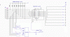
So here's your idea: Control.pdf.
First: I couldn't find 74LS25 so I changed it with SN74HC4002 (again dual
4-input positive NOR gate).
Second: At the triggers' outputs you see "Port#". I'm placing a buffer
(SN74LS541N - Octal Buffer and Line Driver with 3-State Outputs) on each
of the outputs. So that I can send positive impulses to as many switches
as I want. In my case: the greates amount is 4 (MAX333). On each of
the switch inputs there's a pull-down resistor tied to GND.
What's you opinion?