Hello All,
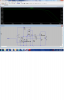
I am working on a Constant current load (adjustable from 250mA-2A) for a project. The load will be batteries around .6V-1.5V I bread boarded the circuit and it worked great. I transferred it over to PCB and not so great. It was a disaster. This is my first mixed signal pcb. Needless to say I didn't pay attention to where signals were routed and I overlapped digital and analog signals. I've since redid the layout. I'm hoping this will keep my analog and digital signals clean not talking to one another. If you all could provide any feedback and pcb layout conflicts that would be greatly appreciated. How could I improve this layout? Would ground plane cuts help with this design? I have attached the pcb file and schematic.
Amir