SnaRf
New Member
Hey all
I am pretty new to electronics, and brand new to the forums.
My highest electronics knowledge is from high school, which is pretty basic..
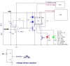
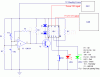
I am about to embark on building this.
(Circuit attached to this post)
I understand what the whole circuit is supposed to do, but I am having trouble reading it.
I can see that the LM339 comparator has V+ on pin 3 and is grounded on pin 12.
It compares the voltage over pins 4 and 5... I think.
The relay has V+ on pins 5 & 6, and apparently on pin 3 as well (Still looking for a pinout)
(so pin 3 will be used to power the LED's)
When the circuit is powered, pins 7 & 8 will be bridged and pins 3 & 4 and the green LED
will be powered
Thus, R5 would be the resistor to stop the LED's from popping...
So, as the temperature picks up, the resistance in TC1 decreases, allowing more
current to flow through it. The goal of VR1 would be to "bleed" some of the current back
to ground(I think). In doing so, it allows you to customize the amount of current reaching
pin 5 on the LM339. Thus customizing your "high" temperature.
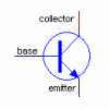
Pin 2 from the LM339 will send a signal to the transistor.
(I am guessing it would be wired up to the collector of the transistor.)
The transistor will then pass the signal on to the relay (pin 1) which will break the
contact between pins 7 & 8 and pins 3 & 4, and make contact between pins 2 & 3
and pins 8 & 9 (pin 9 isn't used though..)
Thus, the green LED will be turned off and the red LED will be turned on.
and the contact will be broken for the "power on signal" wire.
It will then stay in this condition, until the "push to make" switch is pressed to reset the relay,
which will then again break contact between pins 2 & 3 and pins 8 & 9, and make contact
between pins 3 & 4 and pins 7 & 8... right?
What I don't get is the function of R1, R2, R3, R4, Q1, D1 and D2
I am pretty new to electronics, and brand new to the forums.
My highest electronics knowledge is from high school, which is pretty basic..
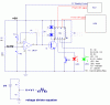
I am about to embark on building this.
(Circuit attached to this post)
I understand what the whole circuit is supposed to do, but I am having trouble reading it.
I can see that the LM339 comparator has V+ on pin 3 and is grounded on pin 12.
It compares the voltage over pins 4 and 5... I think.
The relay has V+ on pins 5 & 6, and apparently on pin 3 as well (Still looking for a pinout)
(so pin 3 will be used to power the LED's)
When the circuit is powered, pins 7 & 8 will be bridged and pins 3 & 4 and the green LED
will be powered
Thus, R5 would be the resistor to stop the LED's from popping...
So, as the temperature picks up, the resistance in TC1 decreases, allowing more
current to flow through it. The goal of VR1 would be to "bleed" some of the current back
to ground(I think). In doing so, it allows you to customize the amount of current reaching
pin 5 on the LM339. Thus customizing your "high" temperature.
Pin 2 from the LM339 will send a signal to the transistor.
(I am guessing it would be wired up to the collector of the transistor.)
The transistor will then pass the signal on to the relay (pin 1) which will break the
contact between pins 7 & 8 and pins 3 & 4, and make contact between pins 2 & 3
and pins 8 & 9 (pin 9 isn't used though..)
Thus, the green LED will be turned off and the red LED will be turned on.
and the contact will be broken for the "power on signal" wire.
It will then stay in this condition, until the "push to make" switch is pressed to reset the relay,
which will then again break contact between pins 2 & 3 and pins 8 & 9, and make contact
between pins 3 & 4 and pins 7 & 8... right?
What I don't get is the function of R1, R2, R3, R4, Q1, D1 and D2

")