Continue to Site

Welcome to our site!

Electro Tech is an online community (with over 170,000 members) who enjoy talking about and building electronic circuits, projects and gadgets. To participate you need to register. Registration is free. Click here to register now.

  • Welcome to our site! Electro Tech is an online community (with over 170,000 members) who enjoy talking about and building electronic circuits, projects and gadgets. To participate you need to register. Registration is free. Click here to register now.

Oscillator in a simple smps

Status
Not open for further replies.

ArivNidunami

New Member
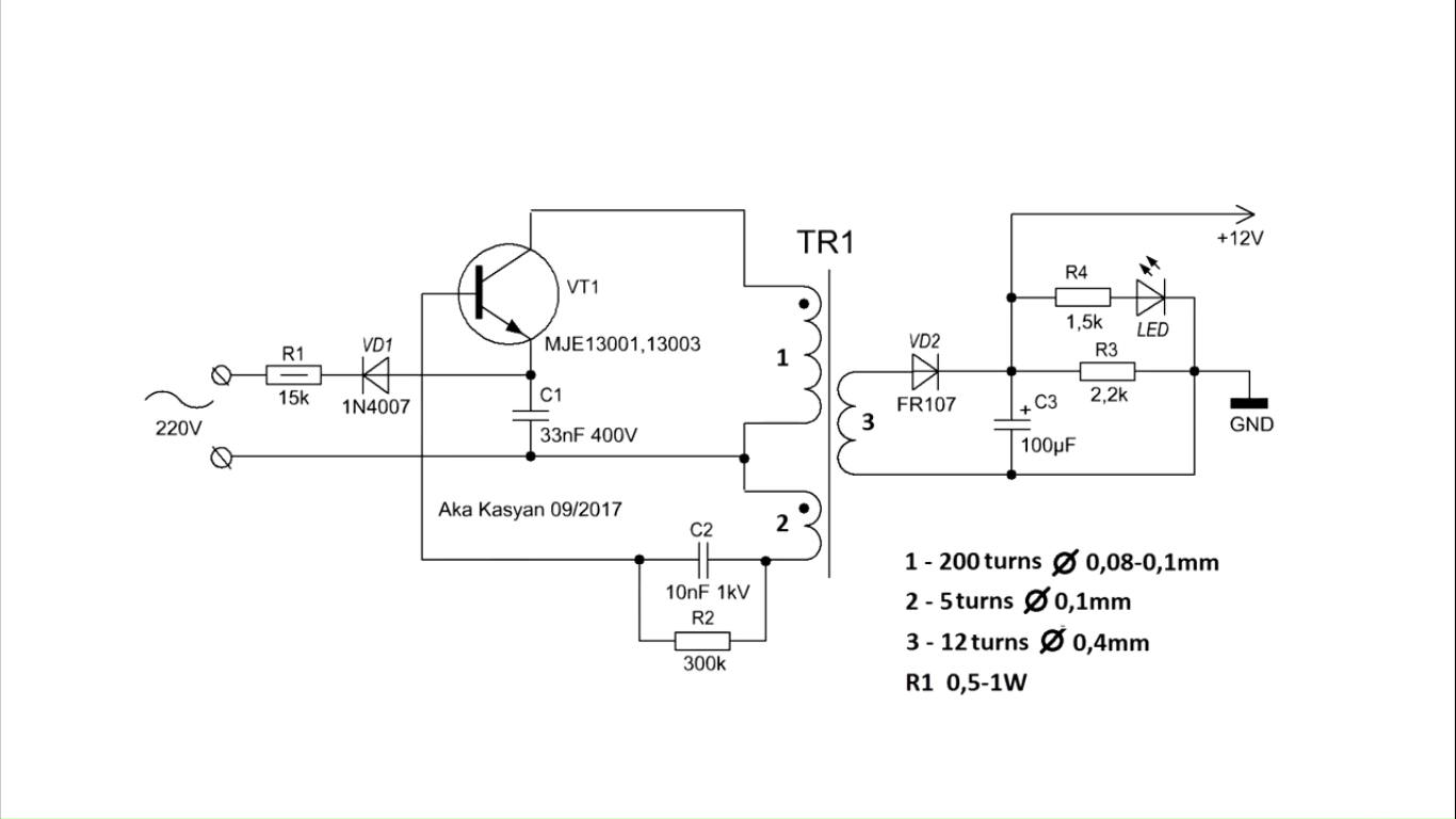
Hi guys, can anyone explain to me how this circuit oscillating? thanks.
df.png
 
As per Nige, as well as however the inductance of the transformer and to a lesser extent C2 will set the oscillation freq.
 
winding 2 provides feedback, R2 provides proper bias for the transistor.
 
First I redrew the schematic. I hate "B-" and upside down drawings. (see left side)
Now I see it is almost what I have done before. (see right side)
What I did, is more L2/L5 from B+ to B-E of the transistor. (same circuit)
I have had to add D3 to reset C2/C4 and I found things better with a small amount of R5 but it is the same circuit.
R2/R4 puts a small amount of current in to the Base of the Transistor. Luck, a discontinuous flyback starts out with zero current so the transistor is easy to turn on. As B+ voltage is applies to L1/L4 a small fraction of this voltage is applies across L2/L5. This pushed up on the Base and really gives the Transistors some base current.
Two thing are happening. 1) the Collector current ramps up and 2) the base current ramps down because of C2/C4. At some point the Base current is too low and the transistor tears open.
At this point the primary flys up above B+ and the Base Drive winding pushed down on the base. This continues until the transformer power is dumped into the secondary winding and the transformer rings back to zero voltage across the primary and secondary(s).
Now C2/4 and R2/4 start the charge up time again.

1582514038851.png

Note: Almost all internet schematics do not work and have errors. (including what I post)
I think the schematic in #1 may be simplified. I looked at a number if the simple 1,2, & 3 transistors PWMs like this and a diode on the Base is very common.
 
Note: Almost all internet schematics do not work and have errors. (including what I post)
not to mention that the primary side is "hot" and should not have any exposed metal surfaces if it can be avoided (most manufacturers these days use plastic isolated TO220 transistor so the heatsink can be grounded (or they use heat sink insulators that can withstand the 1500V isolation requirements). also, with LTSpice, L1, L2, and L3 should also have a K spice directive coupling their mutual inductances as a transformer model.
 
Status
Not open for further replies.

Latest threads

New Articles From Microcontroller Tips

Back
Top