Continue to Site

Welcome to our site!

Electro Tech is an online community (with over 170,000 members) who enjoy talking about and building electronic circuits, projects and gadgets. To participate you need to register. Registration is free. Click here to register now.

  • Welcome to our site! Electro Tech is an online community (with over 170,000 members) who enjoy talking about and building electronic circuits, projects and gadgets. To participate you need to register. Registration is free. Click here to register now.

Open collector comparator pulls up to higher voltage than the pullup voltage!

Status
Not open for further replies.

Flyback

Well-Known Member
Hello,
We are using a TS391ILT open collector comparator.
Its Vdd is 14V
Its output has a 33k pullup to 3V3, and the output goes to a microcontroller input. This microcontroller is supplied by the same 3V3 that the output pulls up to.
On the noninverting pin we have an 8V3 reference voltage.
On the inverting pin we have a square wave which has a frequency of 10ms and goes from zero volts to 13V.
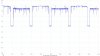
At the output of the comparator, when the output should be pulled up to 3V3…it is instead pulling up to about 3.9V.
Do you think this is due to leakage current from the Vdd pin to the output pin?

TS391ILT datasheet:
https://www.st.com/content/ccc/reso...df/jcr:content/translations/en.CD00001660.pdf
 
How is the Vcc- connected?
 
? add an additional pull down resistor to outp , reduce that 33k atenuate with small resistor 10Ω and less before uC MOSFET input
?? add a feedback (e.g. a minor hysteresis) to your comparator biasing it as if it was an op amp ... reduces need to overdrive it with 13V SW ... ??? assume the input stage PN junctions have BW FW recovery as any diode . . .

the frequency 1/10milliseconds (100Hz) won't show the feature you describe in LTSpice LM393 and CD4049 (poor) component level models
the frequency 10mc (? mega cycles (per second)) . . . oh i forgot - the 39x can do bearly 2MHz
testing 10kc ... 100k ? too fast for 33kΩ
testing 100Hz with miread 33k : 3k3 ... k33 (330Ω) the comparator output stays at 1.9V that is above 1.1V simulated threshold
testing 100k with 3k3 pullup ... nope
...
adding parasitic inductance 2µH and 5pF capacitance to SW 5pF capacitance to +input (8.3V with 1k series resistance)
AND L.pz C.pz in between comparator output and uC input !!! voila even when reducing 8.3V to 50Ω the output rings to 3.6V
... ► 5pF (value of the parasitic capacitance) in between +,- inputs +,GND and OUTP to - input removes that crap ... in simulation (also removed parasitic inductor from OUTP to MOSFET inverter INP) . . . . but now there are pulse edge ringings up to 3.8V . . .

blah blah blah blah blaaah .....

there's some about such in AN4071
________________________________
¯¯¯¯¯¯¯¯¯¯¯¯¯¯¯¯¯¯¯¯¯¯¯¯¯¯¯¯¯¯
(here's what i managed to screw up :woot: -- the mysterious L-s and C-s before R11 & R4 suppose to add wire maze effect ?? -- C1 C2 and C4 are intentional to minimize the maze . . . hopefully:eek:)
9jnRVWxMT7igJaUhavYqOKUkurMr1I72qnMsGM6mMIxxMHCvhTU54gCtxkHfKv0U493Oqz6WRkdfMO3mvpiW6B1mUSGTCrJKJP5CWK2FFf_j_ryB6dr0r9ddrgQNOD4cCDnhSCHSw8Lxs-v00FnCdi2bv6Qhq8fAwqr6vCKMXzTxBH0AY2CRrWfpND7vwqzbJJYVB-N7UGZtzeYBxsit4nh53zh--wwtv2Pcbhzc6nD0DlU_97hx11PmDaQKiku-5JNRdx9srUbxcjUAyJERFqB6Fphv3wJRVrn_h0fTzmkpBRpGPY4vVtXxFeson2LE5ppFyeuqX7JWWQSUGJ-SToWsxYrixYm6dxW1TMbkn9bMC1zrKtitinR0qFg0td7nXX-vLJh-fgmF8jSROzDyVwah72YS6gZR2CYMk0MHnaU9_whMg3ClL3-yrQi-7HdeN-GfXHeFire1AzH4rzepGgXowCXXqgL9FPtCBoSHQPSkyRhCPbNpDPAdD5bb6bZn5UYa6NjM-6Vuu3MKaWLXId1Rv2PHDLLOK_D0aLNtVOVOt83lGHEVU2eTdP7iB_eN_qw8WnzfToSabchp_cM-wYzMqcSc3znV6JufSrZztXGO33LadMtX=w1188-h913-no


it looks the inverting configuration can't do 2MHz
BQ9YpZjDQo1b6j6MA8zxKLhHD07SF5ttXe7SLexzeRaZik8o1S7seee0iLBYvqUn3y9tR-i-eD39LP4cogwv8vRKU3lHADE2ePcSxeVBnBTNm-d4pGfsvYyeD7junwgzRiUfDvvAmlq6u6716o8DKKV_pcsA17OSbU_7p_dNxWP5AKfhB2a4EPQSO_o9Nt-ZnfV8unZklyaMCNi7iXZ907NSG5wovb7SxuyWrXkqaZQY8-JdnIg6rgfSRhtz8Rjd6RFOYqa8Z77flMe0aqsgfTn3zXpQXA7tK-tXyU6l5frivwsspDNdGPoREUO2VJqEbP2Pjfij-rbYSWrhwR5CMGTJoen0U4UeSM61K_TrFpMCs8-c82-rzcPUtKqeTKPtAI6R4R6e5jRvD2ZDwbcRUvVfTS5rJxzR6javrR0Nd93LlKjfi4V_rmKGWrxo86GfoUfd6bAoOFG0Z1ae2uD3xNbVRvxWDOlT18kzoy7cPKjTE3S4ErhtSRieny0h7gO_6Qm-5c6IydLIMOnX9kp2oAqMxjjTWeoNt_ZRX5kyIGggql7FQ_WUwxt2daQ1_ohfPJr85MeOuIpBMiR4kOSoGtcyKRnLFU24OyktRMCEgkFPRb5XvFrJ=w1188-h913-no


the component model a bit differs from the one on datasheet F;X

oZUuGFrW-guxaLRvgipKcKlzkGrp0wvuifPZPI7yXHKKwaEQPD8Kz0g8tfnXf7giIj1JS1hSc6eTsnKs6oxFhvaMVkjHll187rRF-SfUaNzqb8kpwVt1Z6ldEd2SJyEgpU5WW4Xc1Hg_MLPo9LDJ-Gg_lt9bJxfrlgdSqHkVAQfEP6bjM_9S5vEYVCOiaO6L-8g3qVnKLftkg7PrG2eUmbfK0sKh8cZ0w7kK2lrj3CQavIMIn7r7OipOSnX1E9VP6kqrauOUJnq32lTs8OzdTYVlCYW-ZH4pEglnxiFlWcOifgJ_Shp-tlgE8bvslM7QLaWQShtxByag6q2glz_BX7fvrby_TQkvIPWjyHgYZEXYfl-irmvlh7s5jrIwIDKQRcFscEtXHBMNMMZ0zk_YTIfXuQND-IO2lrDpAJzCwA2pPYZptACfF3QhEinJXsKJamfcH9eB8Po6T2DuRoZt9DBhuzisuQC9-PkdMbeANLIcLdR9hnDY-ZtHeXI6V3r8hS--swftJV82KsfH5SnDCQVZASZpsLO9xQ62-taWeegVIxqB4wOlfZrCy1xFeXDxf7nSLPzk3ae-1T4-sZGutJjR81VJ6UVAVd-xnIt9djjb8ncLrLi9=w1265-h530-no

_____________________
2017-04-26 ::
¯¯¯¯¯¯¯¯¯¯¯¯¯¯¯¯¯¯¯¯¯
m0kQWK2jeU98whnjTmwLdrR7m9jQ0kc-sPgNOHtkI0LMl6_BERH1MVXrLDhVN8r79ggCvrk64euaCd4ErKub9Cp4rQYR_9PjS2WKBpt-8_uYoEgtPYoucOdYxS8HEzpjPHMUIKq4notz3mvc4CgCMxMylfDJ_0PvydkNTfyA2ivdV2VUCEhddyMk_Vh1Nn3xSQKioigTpdN2T0-_se3t_gQduA8Mwj058knfmSSCKpIlotC014R31LcI8V-4m0NDqn7-CGsKjoq3vTbXkJ5fQqIliBwE9x36ybY6rQEiGPI2twgn9__D4CYiZtO_QOhTymiPT09_PEPs5nk1h_WEj19o4cffFC1MaqmYEImJF0rFq3I-aS7QFqJnJU3Zjrkf7Qk9Z3stCGrsULArXs5JwRAn5RRzDTuVtnHU3KOgv-46u1QKW5-62hQO8xCzexWvnPe7PxYGZJbJdVZTJfeDnYmH291AEbbK9Qj6s-A1YSoya7sVDnIE3tC5wTJdxRk_CxOsR1OWaXN_rv8rlgkmXqV8W-PKl_NfnZ0UnFjGrmVNB7nfnVqzUxNKuOktTkf3LwOdjCV07OFCozYUW3cgrxjptKTQyoghOSg4YFjgc-8ius_gi6Fn=w1188-h913-no
 
Last edited:
Are you saying 1 or 2 inches of wiring or pc board trace length has 2 uH of inductance?

ak
 
Flyback - after 1,821 posts - no schematic + no scope shots = no good answers.

ak
 
Are you saying 1 or 2 inches of wiring or pc board trace length has 2 uH of inductance?
likely not but to spot problems in ideal simulation that runs up to 1000x more precise than the real life circuit you need to overshoot that much e.g. 2nH in real ???

!! 2016-04-26 :: which is not exactly the truth or not the whole story or not the exact reasoning behind using 2u inductor ::
  • the stat average precision loss from Spice to Real is actually some 10x
  • using small inductors increases simulation times (i don't like to wait)
  • the effect(iveness) of "a fix" for ultra low parasitic'-s can't be adequately studied/spotted
  • the wires(signal lines) in field app.-s actually might be lengthy (it might be also an undershoot)
  • ... there's likely more . . .
 
Last edited:
The scope shot of the comparator's output is attached here.

You can see it pulling up to 3.9V. Actually, I am now more noticing that it only alternately pulls up to 3.9V. Every 10ms it alternates from “Normal” 3v3 otuput, then to “abnormal” 3v9 output. The circuit is grounded to the full wave bridge rectified mains, with no isolation. The PCB is sitting on an earthed heatsink. (on a thin thermal pad).

In other words, the circuits ground is “Neutral” for 10ms, and then it is the negative going “Live” for the next 10ms. (due to the way a full wave bridge rectifier connected to the mains operates) As you know, “Neutral” is approximately earth potential.

I am now thinking that there is some kind of capacitive coupling between the comparator and the earthed heatsink, and that whenever the circuit ground is on that half cycle that represents the negative going live wire, then there is some interaction which makes the comparator’s output go to 3.9V.

Have you come across this before?

Maybe indeed this is not a leakage problem at all.
 

Attachments

  • Comparator output voltage.jpg
    Comparator output voltage.jpg
    151.6 KB · Views: 142
The comparator input is in sync with the mains half cycles
 

Attachments

  • Open collector comparator_1.jpg
    Open collector comparator_1.jpg
    51.3 KB · Views: 144
Thanks, just ran it with no earthing of the heatsink and still get the problem, so it cant be what i thought in my post #9
 
(you don't reference your inputs to anything)
i don't (after admiring some google images of scope plots) like to think it's a scope (( , but also the inequalities in ground balancing trips likely won't produce an overshoot at comparator output))
? divide your OUTP to ??? 100kΩ,200kΩ,100kΩ ? scope the voltage on middle one OR fix OUTP to "high" (3.3V) and get the multi-m and scope reading for comparison
 
Thanks, we are reading this osvervoltage with a TA041 diff probe, and we wonder if it has problems with common mode input range.

TA041 diff probe
https://www.farnell.com/datasheets/22...183.1489787856

I tried adding Common mode choke to AC input of circuit , but that doesn’t solve it and just makes the signal look more noisy.
Strangely the signal looks less noisy when the PCB is raised away from and above the earthed heatsink.
The PCB itself has no earth connection.
Strangely, when the pcb is sitting on the heatsink (with separator pad), the signal looks less noisy when the heatsink is disconnected from earth.

Though whether it looks more noisy or not, the overvoltage every other mains cycle on the comparator output is still there. I changed the pullup from 33k to 2k7 and the overvoltage goes down from 3.9V to about 3.45v

I think a battery scope may be needed to see if this isnt some measurement artifact.?
 
Hello,

You could try a pull down resistor to see how much current it would take to bring it down to 3.300v with the original 33k resistor.

That 0.6v difference does sound like the on chip ESD diode is becoming forward biased and thus limiting the voltage to around 3.9v.

You should hoever check the ground pin of the IC package, marked Vcc- on the data sheet, to make sure it is not being picked up as the output goes high. If the ground pin goes to 0.6v then that would cause a 3.9v output as read back to the real quality ground point.

All voltages like this should be measured from the ground of the IC itself anyway.

If it was leakage from the comparator chip itself that could be proved by providing a steady DC signal into the chip and then making some static measurements with a trusted high impedance DC volt meter. Very simple measurement. If it's an AC type of leakage that would be rare if the current is reasonably high as there is no mechanism for this to happen as far as the data sheet goes, so it would have to be an undocumented issue. In fact there's no mechanism for a DC leakage that high either, unless maybe the chip ESD diode is bad. The ESD diode should have max leakage maybe 1 to 10 na at most i think.

Usually when something like this happens there are experiments you can design to find out exactly what is causing it. It's a thought process similar to the design of the circuit itself where you design a change to the circuit to find out what could be causing it. For this problem using a static DC input would be one such experiment. Disconnecting the output from the following IC stage would be another experiment to make sure it is not coming from the following chip. Isolate the problem to a known source, then hunt it down.
 
The rounding on *both* ends of the 3.9 V hump is a clue to something, but don't know what yet.

I agree that 0.6 V is suspicious, but IMO there's no way there is an ESD diode on and open collector output; having the output drive something at a voltage greater than Vcc is just too common an application.

ak
 
Status
Not open for further replies.

Latest threads

New Articles From Microcontroller Tips

Back
Top